Photoelectronic device and production method of the same
a technology of photoelectronic devices and production methods, applied in the direction of optical waveguide light guides, instruments, optics, etc., can solve the problems of signal distortion, loss of wiring, frequency limit of electric wiring, etc., and achieve the effect of maintaining the degree of freedom in designing
- Summary
- Abstract
- Description
- Claims
- Application Information
AI Technical Summary
Benefits of technology
Problems solved by technology
Method used
Image

Examples
first embodiment
[0041
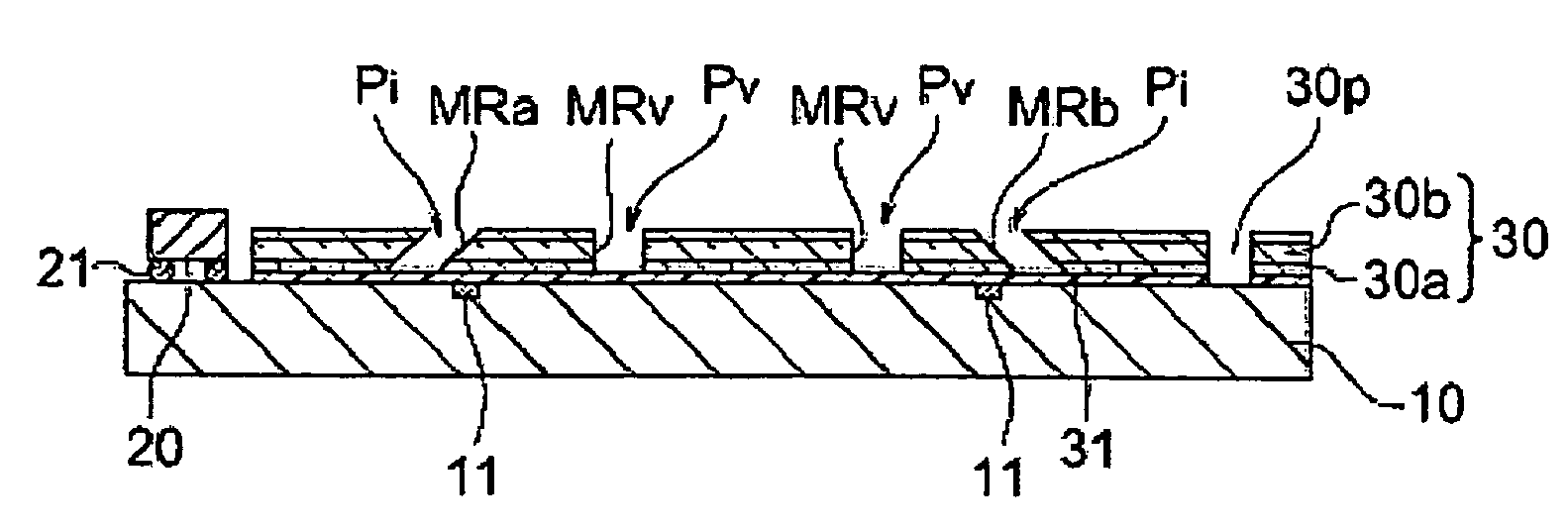
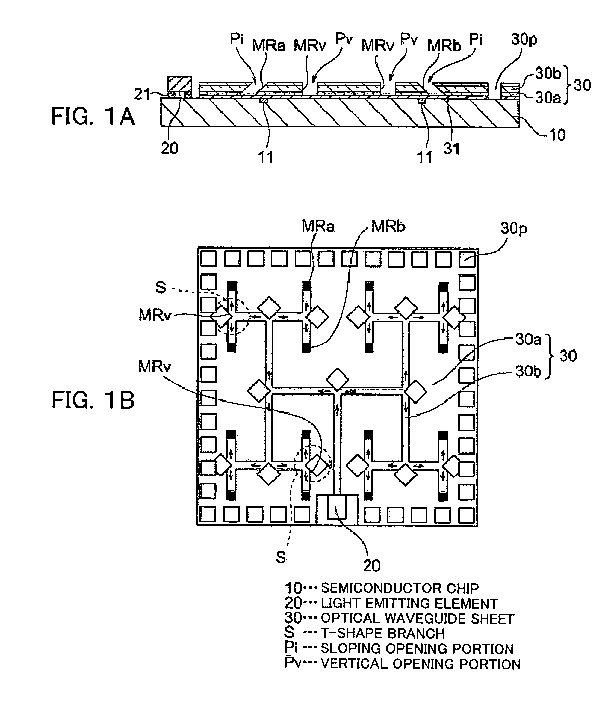
[0042]FIG. 1A is a schematic sectional view and FIG. 1B is a plan view of a photoelectronic device according to a first embodiment of the present invention.
[0043]A light emitting element 20 for emitting a light to be a clock signal, such as a semiconductor laser diode, is mounted on a surface of a semiconductor chip 10, furthermore, on the surface of the semiconductor chip 10, an optical waveguide sheet 30 formed to be a sheet shape, wherein an outer circumference of a core 30b stretching in stripes in the optical waveguide direction is covering with a clad 30a, is adhered by an adhesive layer 31.
[0044]The semiconductor chip 10 is formed with an electronic circuit including a light receiving portion 11, such as a photodiode.
[0045]The light emitting element 20 is mounted on the semiconductor chip 10 so as to be connected to pads of the semiconductor chip 10 via bumps 21.
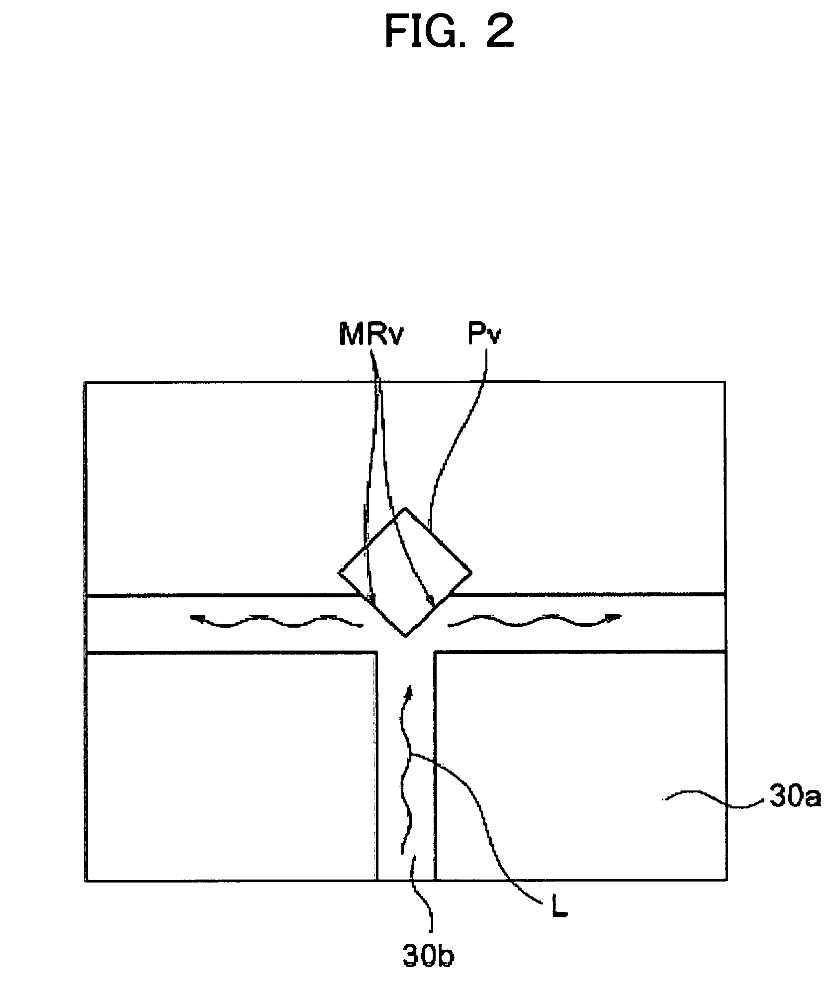
[0046]The optical waveguide sheet 30 is irradiated at its light incident portion of the core 30b with a light ...
second embodiment
[0091
[0092]FIG. 8 is a schematic sectional view of a photoelectronic device according to the second embodiment of the present invention.
[0093]It is configured that a semiconductor chip 10 adhered to an optical waveguide sheet 30 and a light emitting element are mounted on an interposer 60, and a light from the light emitting element 20 is irradiated from the side surface of the optical waveguide sheet 30 to the core. Other configuration than that is substantially the same as that of the first embodiment.
[0094]Namely, the light emitting element 20, such as a semiconductor laser diode, for emitting a light to be a clock signal is mounted on the surface of the semiconductor chip 10 and, further thereon, the optical waveguide sheet 30 formed to be a sheet, wherein an outer circumference of the core 30b stretching in stripes in the optical waveguide direction is covered with a clad 30a, is adhered to the semiconductor chip 10 by an adhesive layer 31.
[0095]The semiconductor chip 10 is for...
third embodiment
[0103
[0104]FIG. 9 is a schematic sectional view of a photoelectronic device according to the third embodiment of the present invention.
[0105]A plurality of semiconductor chips (10a and 10b) are adhered to an optical waveguide sheet 30 and mounted on an interposer 60. Also, a light emitting element 20 is also mounted on the interposer 60, and it is configured that a light from the light emitting element 20 is irradiated to the core from a side surface of the optical waveguide sheet 30. Other configuration than that is substantially the same as that in the first embodiment.
[0106]In the photoelectronic device of the present embodiment, it can be configured that the plurality of semiconductor chips are respectively provided with light receiving portions, and each of the light receiving portions is connected to each of lights divided at the optical waveguide sheet.
[0107]Furthermore, it may be configured that a part or all of the plurality of semiconductor chips is provided with a plurali...
PUM
 Abstract
Description
Claims
Application Information