Method and apparatus for laser cutting and drilling of semiconductor materials and glass

Inactive Publication Date: 2007-02-06
SEMAK VLADIMIR V
View PDF10 Cites 44 Cited by
  • Summary
  • Abstract
  • Description
  • Claims
  • Application Information

AI Technical Summary

Benefits of technology

[0010]The present invention addresses the above noted shortcomings of the prior art by providing a method for laser drilling and laser cutting of semiconductor material or glass in pulsed regime, by which, for a given laser power the rate of material cutting is substantially higher than the rate obtained using conventional laser cutting. The hole or cut produced by the laser-induced removal of material has a reproducible shape, the drilling or cutting does not produce material debris or

Problems solved by technology

During the process of diamond saw cutting, multiple cracks are always produced in the wafer.
This technological step increases the cost of semiconductor chip manufacturing, and has a significant effect on the environment.
The rate of diamond saw cutting is proportional to the semiconductor wafer thickness, and cutting of wafers thinner than 50 micrometers is impossible using a diamond saw.
Additionally, cleaving produces a certain amount of scrap due to chipping of the edges of the cleaved wafer, which increases production cost.
The main challenges are: 1) the high cost of dicing due to the high cost of laser systems and

Method used


Image

  • Method and apparatus for laser cutting and drilling of semiconductor materials and glass
  • Method and apparatus for laser cutting and drilling of semiconductor materials and glass
  • Method and apparatus for laser cutting and drilling of semiconductor materials and glass

Examples


Example

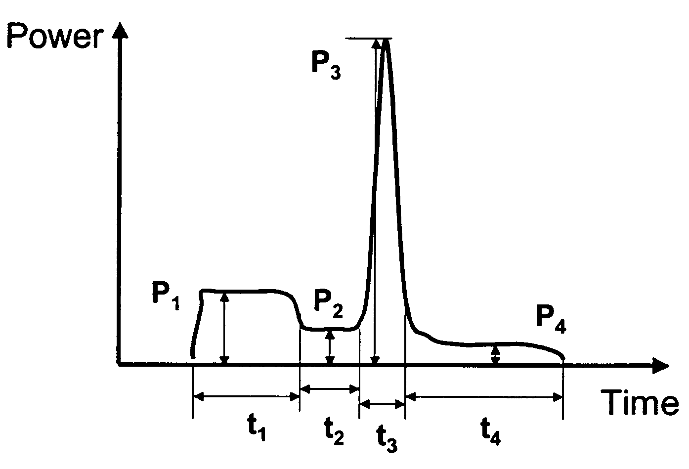
[0029]A preferred embodiment of the present invention comprises two phases. A first phase involves defining the required laser pulse shape and pulse energy via simulation of the laser induced melting of material, keyhole formation, melt ejection, and controlled cooling of the wall of the crater or cut. A second phase includes configuring a laser or lasers in order to produce a numerically predicted pulse shape, beam intensity distribution and pulse energy, and performing drilling or cutting of the material with the predicted laser parameters.

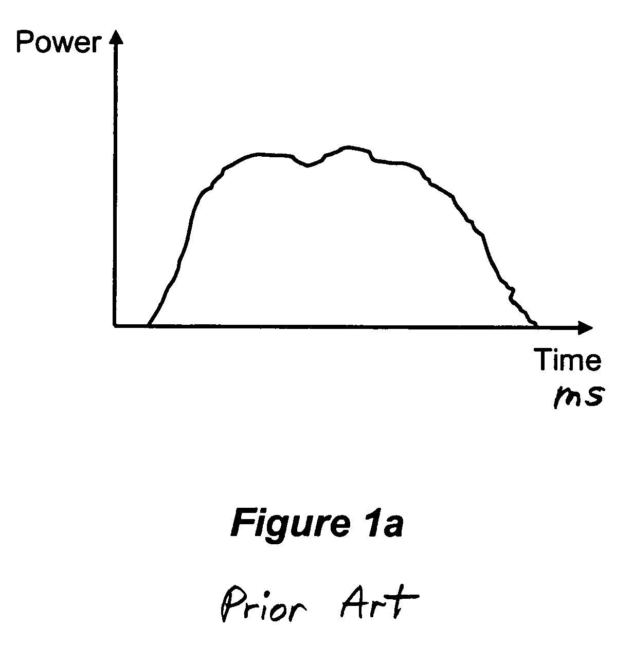
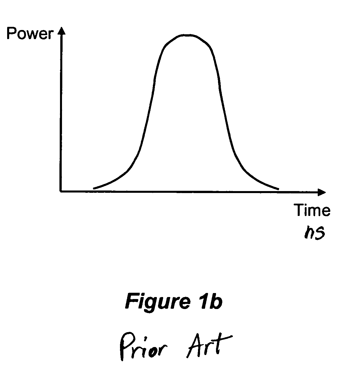
[0030]The invention is based on the following theoretical considerations. Typically, the shape of a laser pulse used for drilling and cutting is as shown in prior art FIGS. 1a, 1b, and 1c. As illustrated, the power of the laser beam increases rapidly, such that melting of the material surface and material ejection occur at the leading front of the pulse. The drilling or cutting occurs during the rest of the laser pulse by the ejection of the mol...


PUM

PropertyMeasurementUnit
Temperatureaaaaaaaaaa
Semiconductor propertiesaaaaaaaaaa

Abstract

A method for laser drilling and laser cutting of semiconductor material or glass in pulsed regime permits, for a given laser power, a rate of material cutting which is substantially higher than the rate obtained using conventional laser cutting. The hole or cut produced by the laser-induced removal of material has a reproducible shape, the drilling or cutting does not produce material debris or spatter deposition around the crater or cut, and the cracking of the crater or cut walls is prevented. The method includes utilization of a unique physical model representing all main physical processes taking place during laser-assisted material deposition, a corresponding mathematical model consisting of equations describing the relevant physical processes, and a computer code used for numerical calculations of the parameters of interest according to the mathematical model.

Description

[0001]This application claims the benefit under 35 U.S.C. 119(e) of the filing date of Provisional U.S. Application Ser. No. 60 / 544,710, entitled Method and Apparatus for Laser Cutting and Drilling of Semiconductor Materials, and filed on Feb. 13, 2004, which application is expressly incorporated herein by reference.BACKGROUND OF THE INVENTION[0002]The present invention relates generally to the field of laser materials processing, and more particularly to technologies related to laser cutting and drilling of semiconductor materials and glass.[0003]Semiconductor Wafer Dicing[0004]Presently, the thickness of the most widely used semiconductor wafers exceeds 200 micrometers. Such thick wafers can be diced using mechanical methods. There are three prevalent methods for mechanical dicing of the semiconductor wafer: diamond saw cutting, scribing and cleaving, and laser cutting. Currently, the majority of wafers are cut using a diamond saw. Scribing and cleaving is utilized only in small v...

Claims


Application Information

Patent Timeline
IPC IPC(8): B23K26/38
CPCB23K26/0604B23K26/063B23K26/0613B23K2201/40B23K26/0622B23K2101/40
Inventor SEMAK, VLADIMIR V.
Owner SEMAK VLADIMIR V
Why Eureka
Try Eureka