Method of manufacturing semiconductor device

a semiconductor device and manufacturing method technology, applied in the direction of light-sensitive devices, electrolytic capacitors, instruments, etc., can solve the problems of material waste, material depletion, and more serious problems, and achieve the effect of improving material utilization efficiency and throughpu

Inactive Publication Date: 2007-02-27
SEMICON ENERGY LAB CO LTD
View PDF18 Cites 21 Cited by
  • Summary
  • Abstract
  • Description
  • Claims
  • Application Information

AI Technical Summary

Benefits of technology

[0008]The present invention is offered in view of the above problems, and it is an object of the present invention to provide a method for manufacturing a wiring, a conductive layer, a display device and a semiconductor device each of which can corresponds to a large sized substrate. A further object of the present invention is to provide a method for manufacturing a wiring, a conductive layer, a display device, and a semiconductor device in which a throughput and efficiency in the use of a material are enhanced.
[0018]The invention in which the conductive layer is formed by ink-jet, namely, by discharging the conductive material has advantages of being excellent at uniformity of the film thickness and the like compared with a screen printing system in which a thin film (typically, an electroluminescent layer) is formed by applying a solution using a printing roll or a relief printing in which a pattern to be printed is engraved, and baking.
[0019]According to the present invention, the treatment is performed under reducer pressure. As used here in, the term “under reduced pressure” refers to under the pressure which is reduced so as to be lower than the atmospheric pressure. And it may set at from 1×10² to 2×10⁴ Pa (preferably, from 5×10² to 5×10³ Pa), and further reduced pressure, it may set at from 1 to 5×10⁴ Pa (preferably, form 1×10² to 1×10³ Pa) when the atmosphere is filled with nitrogen, rare gas, or other inert gas. By setting under reduced pressure, the volume of the solvent is reduced with constantly volatilizing the solvent from a droplet until the droplet arrives to the thin film over the substrate. Therefore, the subsequent heat treatment can be carried out in a shorter time. Further, the steps of the subsequent heat treatment can be omitted.
[0021]According to the present invention having the above-described constitution, a wiring and a conductive layer can be easily formed over the large sized substrate having a side of over one meter long. Since only the quantity needed of the material is discharged, and the small amount of the wasted material is left, the efficiency in the use of a material can be enhanced and manufacturing cost can be reduced.
[0022]In addition, the steps of exposure and development can be significantly reduced since the mask is unnecessary. Plural thin films of such as an electroluminescent layer of a light emitting element and an electrode can be successively formed by changing a composition discharged form an ink head or changing an ink head filled with the composition. As a result, a throughput is increased and productivity can be enhanced. Since a mask for the exposure becomes unnecessary, a circuit wiring inputted into a personal computer and the like can be rapidly manufactured.
[0023]According to the present invention in which the conductive layer is formed under reduced pressure, the generation of the dust added to a resist pattern and the reforming of the surface in which the surface of the object to be processed is oxidized can be prevented. Further, a throughput can be enhanced since heat treatment can be selectively performed only over the region in which the conductive layer is formed according to the present invention in which the heat treatment is performed by a laser or a lamp.

Problems solved by technology

In addition, in the case of performing the etching treatment, a throughput is degraded since a step of manufacturing a mask is required.
Further, some materials are wasted since the etching treatment is performed in order to make a desired shape after forming the conductive layer over the whole surface.
These problems become more serious when a wiring is formed over the large sized substrate having a side of over one meter long.

Method used


Image

  • Method of manufacturing semiconductor device
  • Method of manufacturing semiconductor device
  • Method of manufacturing semiconductor device

Examples


embodiment mode 1

[Embodiment Mode 1]

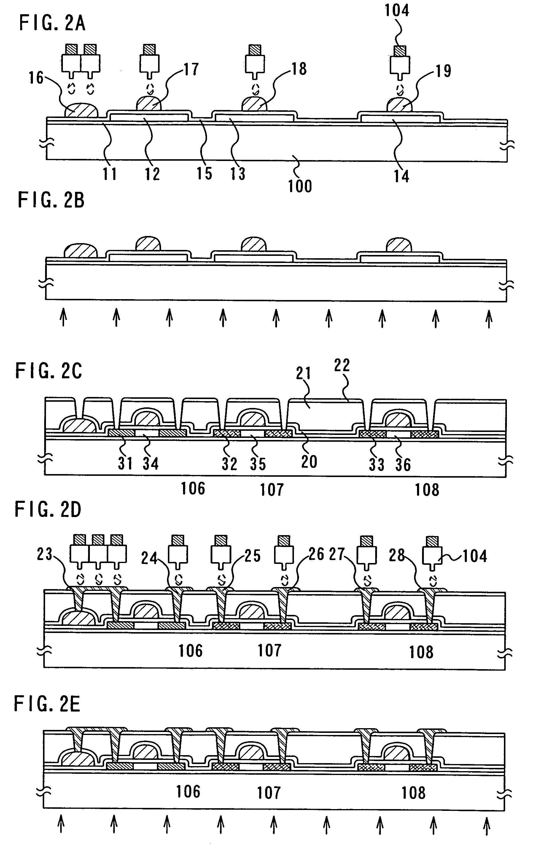
[0042]The embodiment mode of the present invention is described in detail with reference to FIGS. 1 to 4. However, as is easily known to those skilled in the art, the mode and the detail of the present invention are not limited to the following description and can be variously changed without departing from the purpose and the range of the present invention. Therefore, the present invention is not interpreted while limiting to the following description of the embodiment mode. The same symbol is used to the one which indicates the same among the different drawings in the composition of the present invention described below. Here, manufacturing steps of forming an n-channel type TFT (for switching) and forming two p-channel type TFTs (for driving) over the same substrate by using the present invention are described.

[0043]A flexible substrate typified by a glass substrate and a plastic substrate and the like each of which can withstands the processing temperature of ...

embodiment mode 2

[Embodiment Mode 2]

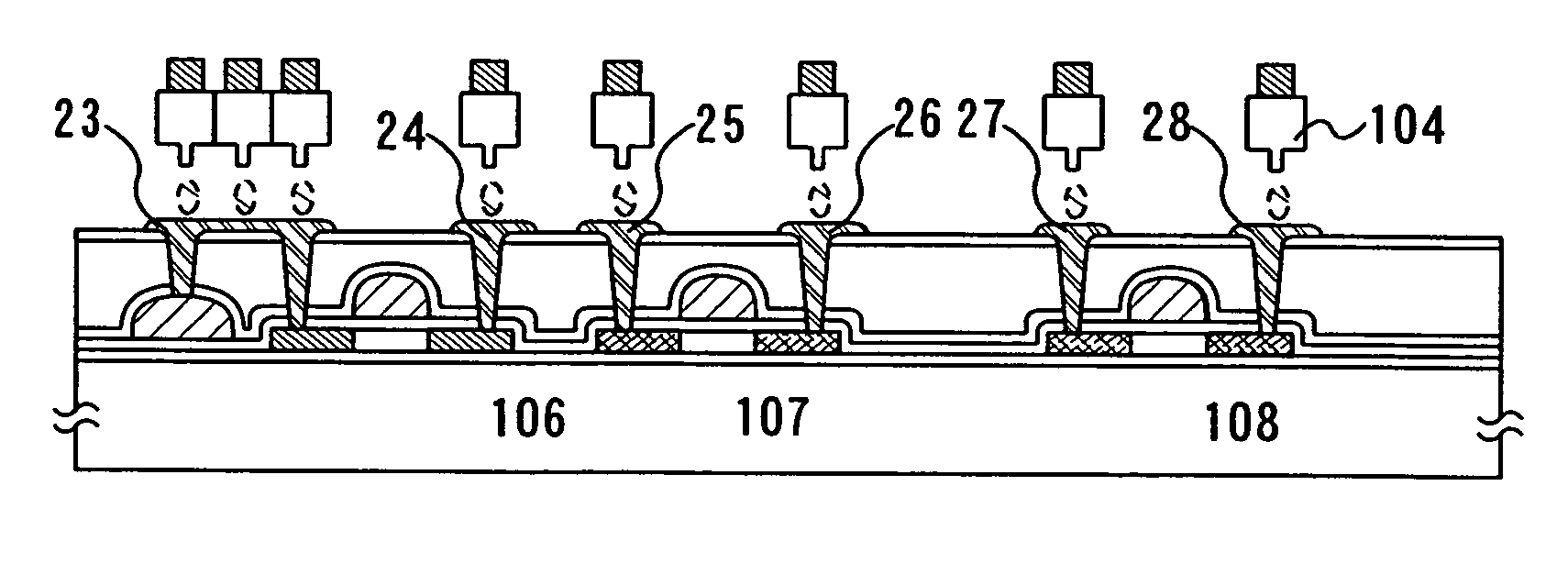
[0081]Embodiment mode of the present invention is described with reference to FIGS. 6A to 6C and 7A to 7E. Here, a manufacturing step of forming an n-channel type TFT (for switching), a p-channel type TFT (for driving), and a capacitor element in the same substrate is described.

[0082]First, a base film 11, a semiconductor layers 12 and 13, and a gate insulating film 15 are formed over a substrate 101 in sequence in the same way as that of Embodiment Mode 1 (FIG. 7A).

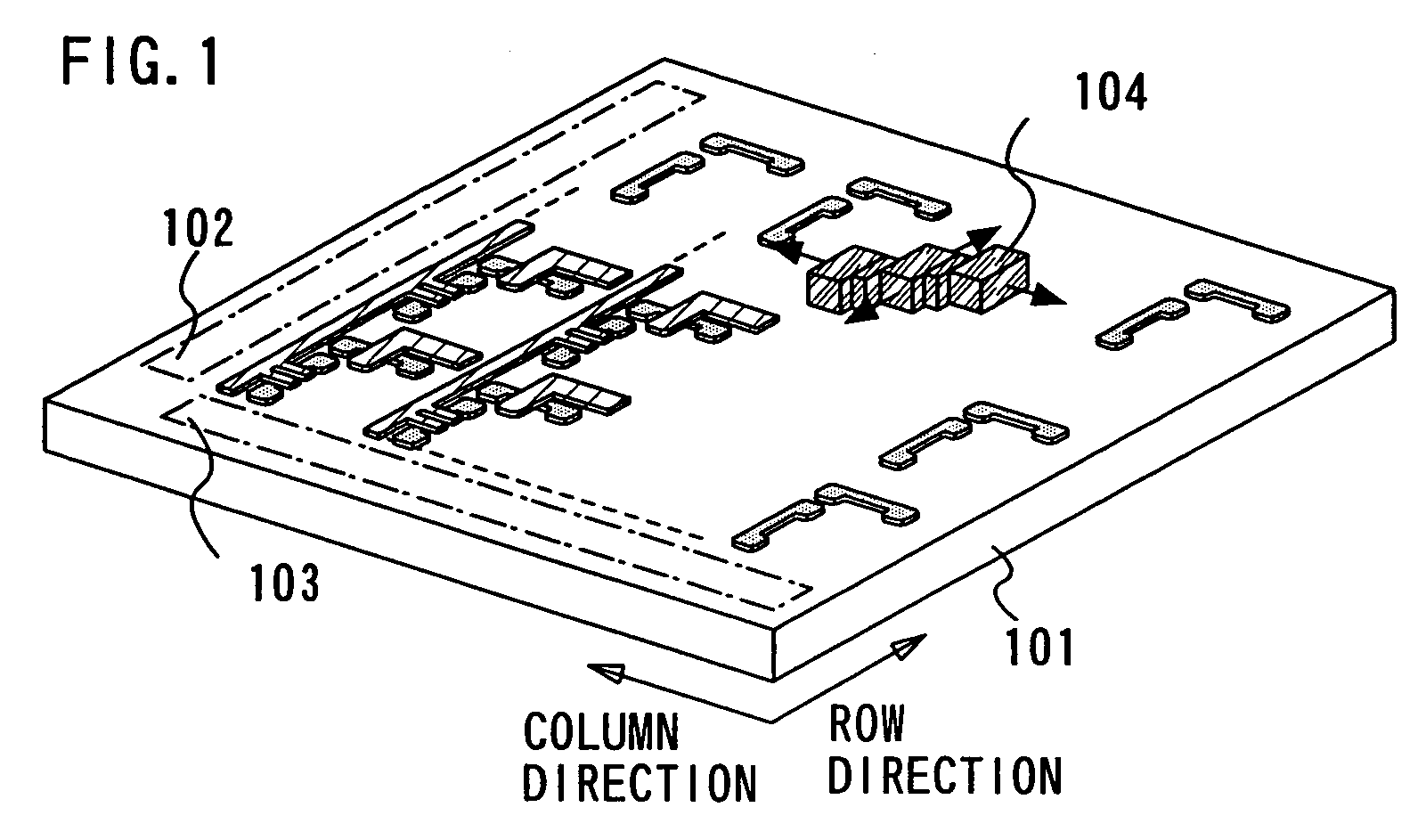
[0083]Subsequently, the first conductive layers (gate wirings, gate electrodes,) 56a to 59a are formed under reduced pressure by ink-jet. The perspective view is shown in FIGS. 6A to 6C and the cross sectional view is shown in FIG. 7A.

[0084]Although not shown in the drawings, a nozzle included in an ink head 104 is preferably arranged in a line in columns. According to this, the first conductive layers 56a to 59a can be formed only by scanning the ink head 104 once in rows on a substrate 101. The compo...

embodiment mode 3

[Embodiment Mode 3]

[0092]In this present embodiment mode, a liquid crystal display panel made by a transistor which is composed of an amorphous semiconductor (amorphous silicon) is described with reference to the drawing. The present invention can be applied to the formation of gate and source wirings, a drain wiring, and the like.

[0093]A substrate 101 is formed of various materials such as glass, quartz, a semiconductor, a plastic, a plastic film, metal, a glass epoxy resin, and ceramic. Conductive layers 557 and 558 are formed over the substrate 101 by ink-jet, that is by discharging a composition having known conductivity under reduced pressure (FIG. 14A). According to the present invention in which the conductive layer is formed by ink-jet, efficiency in the use of a material can be widely enhanced since the conductive layer can be formed only on the desired area.

[0094]The heat treatment is performed over the substrate in which the conductive layers 557 and 558 are formed within...


PUM

PropertyMeasurementUnit
pressureaaaaaaaaaa
pressureaaaaaaaaaa
temperatureaaaaaaaaaa

Abstract

To provide a method for manufacturing a wiring, a conductive layer, a display device, and a semiconductor device, each of which can meet a large sized substrate and which is manufactured with a higher throughput by using a material efficiently, the conductive layer is formed over the substrate having an insulating surface by discharging the conductive material, and heat treatment is performed by a lamp or a laser beam over the conductive layer. Furthermore, the conductive film is formed under reduced pressure according to the present invention.

Description

BACKGROUND OF THE INVENTION[0001]1. Field of the Invention[0002]The present invention relates to a method for manufacturing a wiring, a conductive layer and a display device, more particularly, the present invention relates to a method for manufacturing a wiring, a conductive layer, and a display device by using ink-jet.[0003]Further, the present invention is related to a method for manufacturing a wiring, a conductive layer, a display device, and a semiconductor device by using a method of discharging a conductive material.[0004]2. Description of the Related Art[0005]A thin film transistor (hereinafter referred to as a TFT) formed by using a thin film of an insulating surface is widely applied to an integrated circuit and the like, and is often used as a switching element. Particularly, a display panel using the TFT has been widely used for a large sized display device, therefore, high definition, high aperture ratio, high reliability and a larger screen are increasingly required.[...

Claims


Application Information

Patent Timeline
Patent Type & Authority Patents(United States)
IPC IPC(8): H01L21/00G02F1/1362H01L21/288H01L21/768H01L21/77H01L21/84H01L27/12H01L27/13H01L27/32H01L51/00H01L51/40H01L51/56
CPCH01L21/288H01L21/76838H01L21/76877H01L27/1255H01L27/1292G02F1/136286H01L21/6715H01L51/0004H01L51/0021H01L51/56H01L27/3244H10K71/13H10K59/12H10K71/60H10K71/00
Inventor YAMAZAKI, SHUNPEIWATANABE, YASUKOARAI, YASUYUKI
Owner SEMICON ENERGY LAB CO LTD
Why Eureka
Try Eureka