Wiring glass substrate for connecting a semiconductor chip to a printed wiring substrate and a semiconductor module having the wiring glass substrate

a technology of wiring glass and semiconductor chips, which is applied in the direction of printed circuit aspects, printed element electric connection formation, dielectric characteristics, etc., can solve the problems of low planarity and high cost of ceramics, and the pitch of pins has become more difficult to connect the lead frame to the printed wiring board withou

Inactive Publication Date: 2007-02-27
RENESAS TECH CORP
View PDF10 Cites 31 Cited by
  • Summary
  • Abstract
  • Description
  • Claims
  • Application Information

AI Technical Summary

Benefits of technology

[0030]Eleventh means for accomplishing the objects of the invention is that the conductive material contains at least a conductor, crystallized glass, low melting point glass, a nucleus formation material or filler inhibiting grain growth of the conductor. The composition ratio is not particularly limited and a suitable composition may well be selected. To reduce an electric resistance of via-hole portions, however, 20 to 82.5% by volume of crystallized glass is preferably contained on the basis of the sum of the conductor and the crystallized glass.
[0038]Seventeenth means for accomplishing the objects of the invention is a glass substrate having a plurality of through-holes formed at predetermined positions and an oxide formed on a surface of the through-holes. The oxide preferably contains any element of Ti, Al, Zr, Fe, Sm and Pr. The oxide is preferably a film having a thickness of 0.2 to 1.5 μm. When SiO2 contained in the glass substrate is allowed to react with the oxide, cracks occurring due to machining can be repaired.

Problems solved by technology

As the number of pins of the chip has become greater, a pin pitch has become narrower, and it has become more difficult to connect the lead frame to the printed wiring board without short-circuiting the lead frame.
Ceramics are generally used as a packaging substrate material of the semiconductor chips the integration density and function of which have become higher, but the ceramics are not free from the problems such as low planarity and high cost.
When electrodes are formed inside via-holes formed in a packaging substrate by a prior art method, the following problems may develop in the method that uses a conductive paste and in the method that uses sputtering in combination with plating.
Therefore, it is difficult in some cases to form the electrode inside the via-hole when the conductive paste of the prior art is used.
When the foundation electrode is formed on the inner wall surface of the via-hole of the packaging substrate, however, sputtering must be carried out from both upper and lower surface sides of the substrate and the electrode formation is troublesome and time-consuming.
The prior art technology has not taken sufficiently the strength of the glass substrate into consideration.
When the thickness of the substrate is increased to suppress such a drop, the package cannot be rendered compact and the time required for forming the through-holes becomes longer.

Method used


Image

  • Wiring glass substrate for connecting a semiconductor chip to a printed wiring substrate and a semiconductor module having the wiring glass substrate
  • Wiring glass substrate for connecting a semiconductor chip to a printed wiring substrate and a semiconductor module having the wiring glass substrate
  • Wiring glass substrate for connecting a semiconductor chip to a printed wiring substrate and a semiconductor module having the wiring glass substrate

Examples


embodiment 1

[0095]First, the invention will be explained.

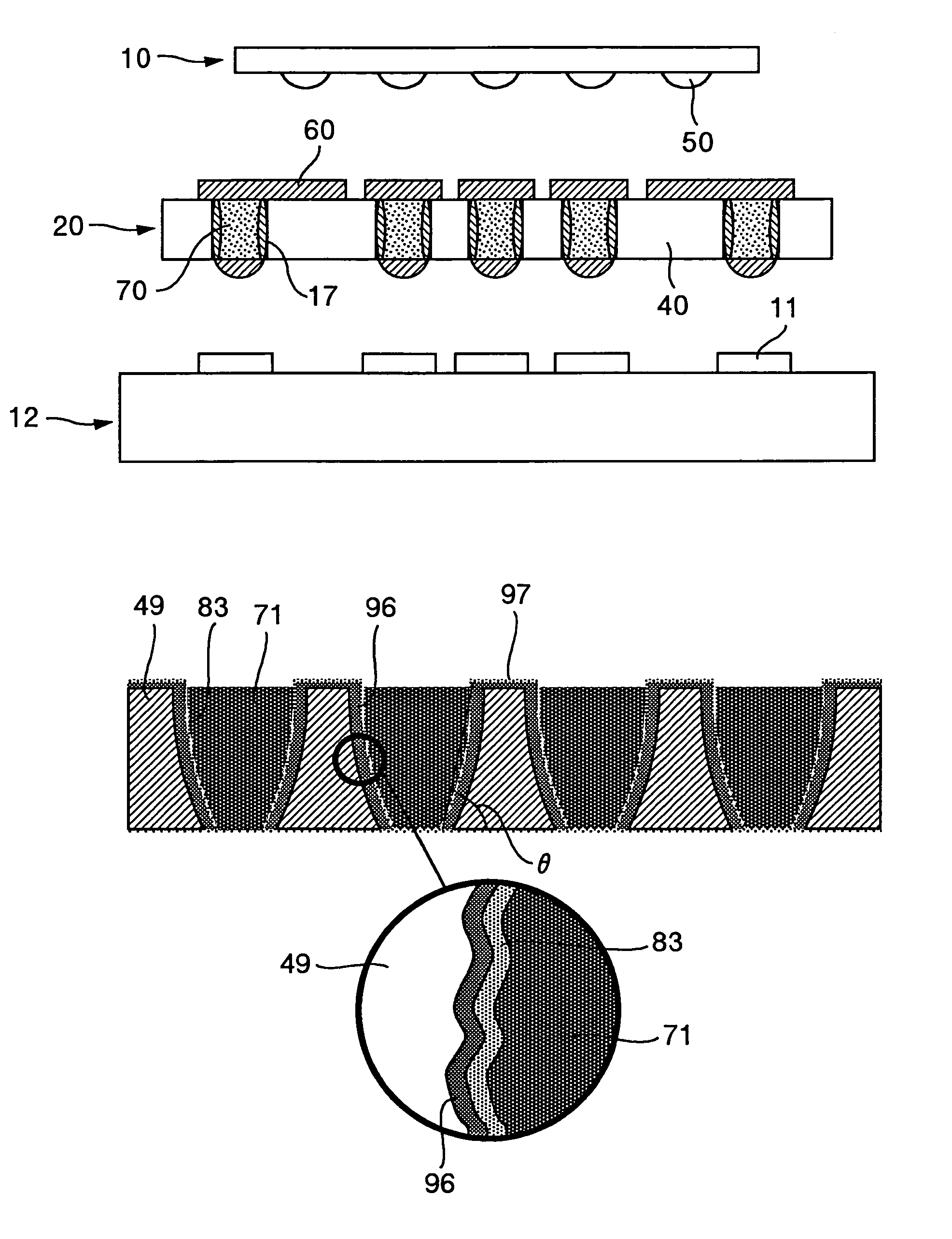
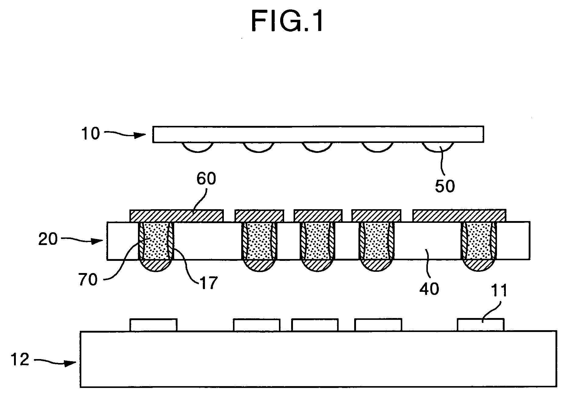
[0096]FIG. 1 shows a wiring connection glass substrate of the invention. This wiring connection glass substrate (wiring glass substrate) 20 is for connecting a bare chip 10 to the upper side in the drawing and a printed wiring substrate 12 to the lower side in the drawing. The kind of glass of a glass substrate 40 as a base of the wiring connection glass substrate 20 is not particularly limited. However, because alkali components contained in glass are likely to precipitate to the surface, those types of glass which contain small alkali components such as alkali-free glass, borosilicate glass, aluminosilicate glass, lithium silicate glass, etc are preferred.

[0097]It is also possible to use quartz glass, though the cost somehow increases, and soda glass that is advantageous in the cost so long as it can suppress precipitation of the alkali components. Holes 17 are bored in the wiring connection glass substrate 20 and penetrate through the ...

embodiment 11

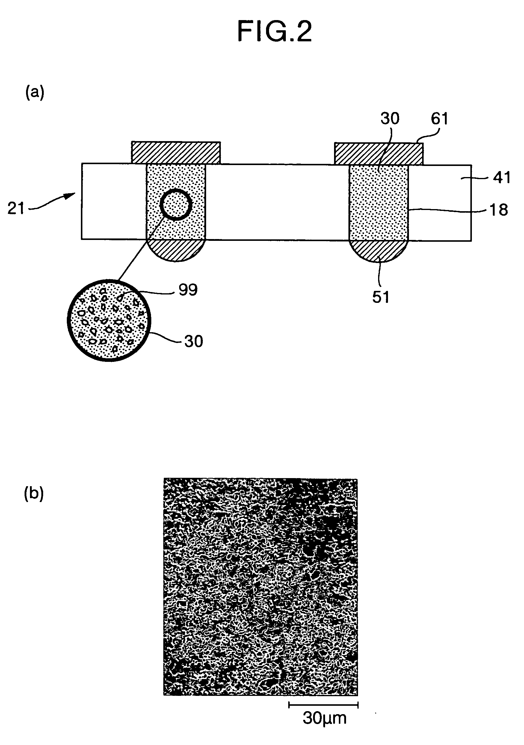
[0102]FIG. 2(b) shows a surface photograph of the via-hole electrode 70. The electrode is found porous as shown in FIG. 2(b). The porous electrode has the pores (void) 99 and fine holes. The porosity of the pores 99 is not particularly limited but is preferably greater than the porosity of pores of the electrode used for the wiring 61 and the bump 51. Incidentally, the method of forming the porous electrode will be explained in later-appearing

[0103]The formation of the bump 51 to be electrically connected to the printed wiring substrate 12 may either use as such the conductive material 30 for forming the via-hole electrode 70 or may use plating. The formation of the wiring 61 to be electrically connected to the bare chip 10 may either use as such the conductive material 30 for forming the via-hole electrode 70 or may use plating in the same way as described above. Plating may be either electrolytic plating or electroless plating.

[0104]FIG. 3 shows deflective strength of a non-etched...

embodiment 2

[0107]Next, the invention will be explained.

[0108]FIG. 4(a) is an enlarged view of a via-hole portion of a wiring connection glass substrate (wiring glass substrate) 21 according to the invention. Each of the holes 18 is formed by laser machining, machining, chemical cutting, etc in the same way as described above and the shape of the holes is not particularly limited.

[0109]Referring to FIG. 4(a), a porous conductive material 30 exists at a center inside each of the holes 18 and a layer of low melting point glass 80 exists inside or on a surface of pores 99. A plurality of pores 99 is scattered inside the conductive material 30. The conductive material 30 is a metal and an alloy of Pt, Au, Ag, Cu, Al, Cr and a solder material in the same way as described above. The low melting point glass 80 is for bonding the inner wall surfaces of the holes 18 formed in the glass substrate 41 and the conductive material 30 or for reinforcing the inside of the conductive material.

[0110]The low melt...


PUM

PropertyMeasurementUnit
temperatureaaaaaaaaaa
Young's modulusaaaaaaaaaa
thicknessaaaaaaaaaa

Abstract

A wiring glass substrate includes a glass substrate formed of glass and having a plurality of holes formed at predetermined positions, bumps so formed as to be connected to a conductive material filling the holes and wirings formed on a surface opposite to a surface having the bumps formed thereon and electrically connecting a plurality of connection terminals arranged in intervals different from intervals of the holes to the conductive material. The shape of the conductive material is porous and porous electrodes are bonded to the inner wall surfaces of the holes by an anchor effect to increase the strength of the glass substrate.

Description

TECHNICAL FIELD[0001]The invention relates to a mounting substrate for a module, for mounting a plurality of bare chips in a high density. More particularly, the invention relates to a wiring glass substrate in which a conductor is formed inside via-holes (through-holes), a manufacturing method of the wiring glass substrate, a conductive paste and a semiconductor module used for the wiring glass substrate and a method of forming a wiring substrate and a conductor.BACKGROUND ART[0002]In semiconductor chips (hereinafter abbreviated as “chips”) such as memory LSI (Large Scale Integrated circuits) and logic LSI that are formed on a silicon substrate and diced, electrodes of the chip must be electrically connected to wirings of a printed wiring board. According to a prior art technology, the chip is connected to a lead frame as is then sealed, and a casing in which the chip is sealed (hereinafter called “chip package”) is connected to the printed wiring board.[0003]As performance of the ...

Claims


Application Information

Patent Timeline
Patent Type & Authority Patents(United States)
IPC IPC(8): H01L23/053H01L21/48H01L23/498H05K1/03H05K1/11H05K3/40H05K3/42
CPCH01L21/486H01L23/49816H01L23/49827H05K3/4061H05K3/426H01L2224/48228H01L24/45H01L2224/45144H01L23/49883H01L2224/16H01L2224/48091H01L2224/48227H01L2924/0102H01L2924/01046H01L2924/01057H01L2924/01063H01L2924/01078H01L2924/01079H01L2924/09701H01L2924/15311H01L2924/19011H01L2924/19041H01L2924/19104H01L2924/19105H01L2924/30107H05K1/0306H05K1/113H05K2201/0116H05K2201/0367H05K2201/09563H05K2201/09581H05K2201/09827H05K2201/09981H01L24/48H01L2924/01019H01L2924/01067H01L2924/01068H01L2924/00014H01L2924/12042H01L2924/14H01L24/49H01L2224/49175H01L2924/00
Inventor SHIONO, OSAMUISHIKAWA, TAKAONAMEKAWA, TAKASHISUZUKI, YASUTAKANAITO, TAKASHIYAMAMOTO, HIROKIKAMOTO, DAIGOROTAKAHASHI, KENSEGAWA, TADANORISATO, TOSHIYAMIWA, TAKAOMOTOWAKI, SHIGEHISA
Owner RENESAS TECH CORP
Why Eureka
Try Eureka