Lateral temperature equalizing system for large area surfaces during processing

a technology of surface temperature and lateral heat exchange, which is applied in the direction of coatings, chemical vapor deposition coatings, electric discharge tubes, etc., can solve the problems of inability to easily compensate local and/or lateral temperature variations by such techniques, and the temperature across the surface of the wafer is not uniform, etc., to achieve rapid stabilization of temperature, reduce the effect of lateral heat flow and small changes in the head

Active Publication Date: 2007-03-27
BE AEROSPACE INCORPORATED
View PDF6 Cites 410 Cited by
  • Summary
  • Abstract
  • Description
  • Claims
  • Application Information

AI Technical Summary

Benefits of technology

[0011]The underlying wicking layer and the spaced apart short wicking columns are spaced so that they are in close thermal coupling relation to all areas of the wafer. Higher temperature at any localized area of the wafer causes rapid stabilization of temperature in that area because of the proximity of sites at which vaporization occurs to one or more wicking posts and the interspersed condensation posts. All the posts have short path lengths to the pool of thermal transfer fluid. Gravitational forces are such that, given the shallow liquid pool, liquid will flow readily with exceedingly small changes in head. This action forces a high lateral heat flow if any temperature differences come into existence. Vapor movement occurs readily as well since there is little to impede flow of vapor in the lateral direction.
[0012]In a more particular example of a system in accordance with the invention, the wicking assembly on the top of the chamber is formed as a horizontal array of sintered metal plugs having intermeshed hexagonal caps or upper surfaces, and depending short wick posts or columns depending from the underside of the cap. At the lower half of the chamber, the condensation assembly is formed as an array of hexagonal conductive plugs with upstanding posts, interdigitated relative to the short wick elements as described above. A patterned sheet metal spring element fitted between the two assemblies has holes through which the upstanding conductive plugs can extend, and contains individual leaf springs formed therein which contact the underside of the depending wicking elements. The sheet metal spring plate thus both holds the conductive plugs in position under downward pressure, and urges the sintered metal plugs upwardly to maintain contact with the underside of the pedestal. In addition, the temperature equalization structure can be reinforced across its surface by strengthening posts which can support the pedestal against gas pressures and provide conduits for thermal transfer gases, wafer removal pins and the like which can function to aid removal of the wafer.

Problems solved by technology

Wafers of this size present problems not heretofore encountered, as to assuring uniformity of the individual patterns in the array wafer.
The total amount of thermal energy to be removed from the wafer may be of the order of several kilowatts, so that it is to be expected, with a 300 mm wafer, that temperature across the surface of the wafer will not be uniform.
As wafer sizes increase, however, as with 300 mm diameter wafers now being produced, local and / or lateral temperature variations cannot readily be compensated by such techniques.
The heat transfer gas flowing in the interface spaces is not readily capable of equalizing temperatures laterally as well as extracting thermal energy.
The semiconductor wafer processing context is particularly demanding in terms of technical requirements and economic benefits.
Standing alone, these devices have potential for meeting specific individual needs, but they do not suggest a solution to the lateral equalization problem presented by large semiconductor wafers.
Although a number of reflux devices are known, such devices do not suggest solutions to the problem of equalizing the temperature of a large semiconductor wafer that is being cooled.
The main problem with applying heat pipes in systems that need tight coupling of heat source to sink is their difficulty in transferring large amounts of heat over long distances.
Unfortunately the pressure drop undergone by the liquid as it travels along the wick is inversely proportional to the same distance squared.
It also means that there is a limit to the distance that a given area of wick can transport an amount of heat with a given temperature difference.

Method used


Image

  • Lateral temperature equalizing system for large area surfaces during processing
  • Lateral temperature equalizing system for large area surfaces during processing
  • Lateral temperature equalizing system for large area surfaces during processing

Examples


Embodiment Construction

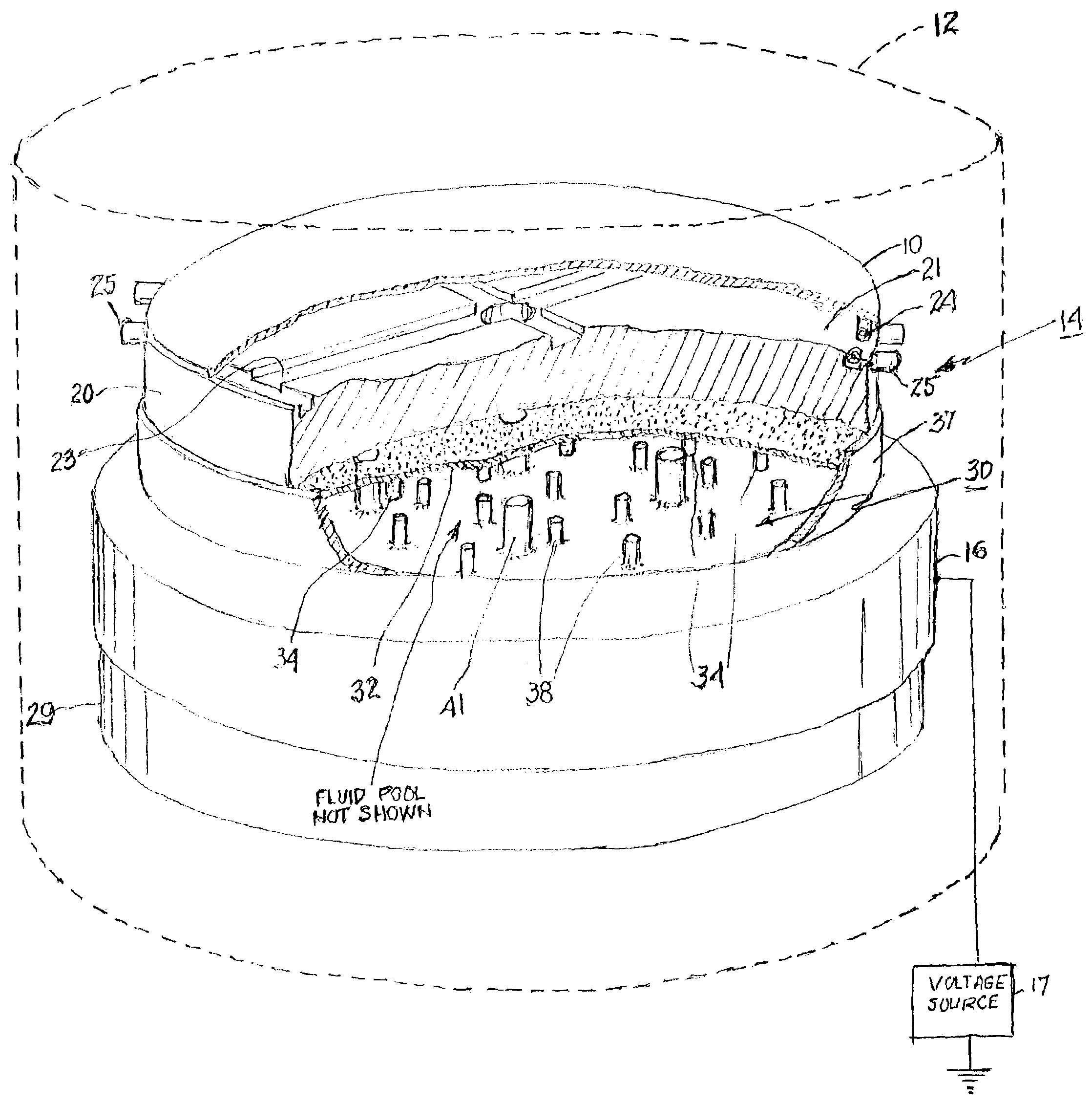
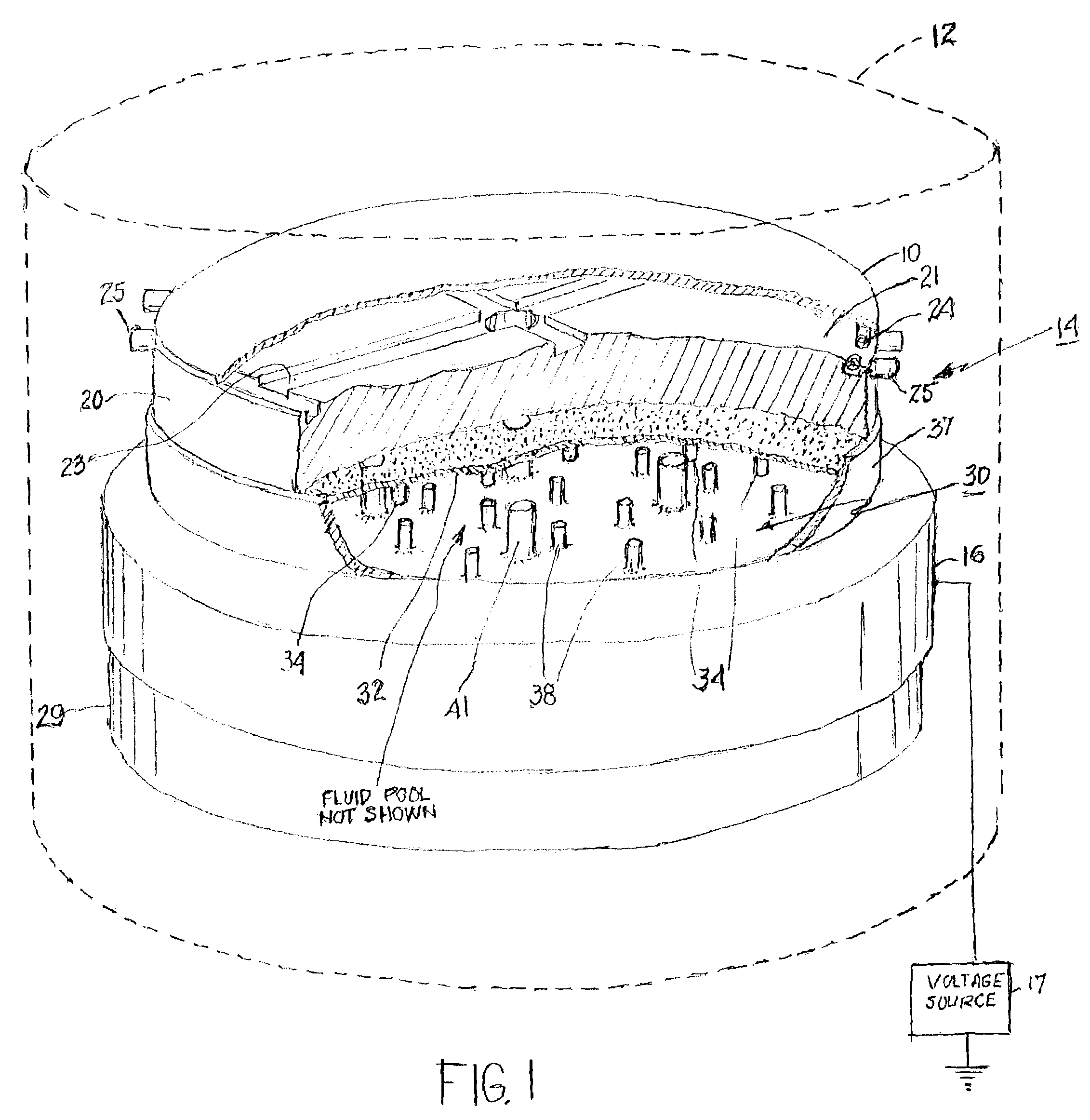
[0020]A system in accordance with the invention, referring now to FIG. 1, is compatible with and complementary to electrostatic chuck systems of the type generally described above. While the system may be employed with any size wafer (substrate), it is uniquely adapted to resolving the critical heat distribution problems encountered with the large 300 mm diameter wafers. The example of FIG. 1 depicts a 300 mm semiconductor wafer 10 in a process chamber 12, indicated only by dotted lines, in which a high energy etching step, such as plasma etching, is to be effected. No disclosure of a specific example or details are needed, as to the wafer holding structure, in view of the state of the art. The electrostatic chuck device 14 on which the wafer 10 is precisely mounted comprises a cathode base 16 that is charged in a desired polarity by a voltage source 17, and an uppermost pedestal (also sometimes called a chuck or platen) 20 with a surface 21 having patterned depressions, such as gro...


PUM

PropertyMeasurementUnit
diameteraaaaaaaaaa
temperatureaaaaaaaaaa
pressureaaaaaaaaaa

Abstract

In many processes used in fabricating semiconductors the wafer is seated on the top surface of a pedestal and heated in a high energy process step, such as plasma etching. The pedestal, chuck or platen may be cooling but the wafer gradually heats until the process can no longer continue. Where large, e.g. 300 mm diameter, wafers are being processed the temperature level across the wafer is difficult to maintain substantially constant. In this system and method the lateral temperature distribution is equalized by a heat sink structure in a chamber immediately under the wafer support on top of the pedestal. A number of spatially distributed wicking posts extend downwardly from a layer of wicking material across the top of the chamber, into a pool of a vaporizable liquid. At hot spots, vaporized liquid is generated and transported to adjacent condensation posts extending up from the liquid. The system thus passively extracts heat to equalize temperatures while recirculating liquid and assuring adequate supply. The free volume above and within the liquid, and the short distances between posts, assure adequate heat transfer rates.

Description

FIELD OF THE INVENTION[0001]This invention relates to systems for supporting and laterally equalizing the temperature of surfaces during heating processing steps, and more particularly to systems for equalizing temperatures across the surface of large area semiconductor wafers.[0002]The development of semiconductor processing technology has consistently tended, for economic and technical reasons, to use increasingly larger semiconductor wafers, in order to multiply the number of individual patterns that may be disposed on the surface of the wafer and thus processed concurrently. In the current state of the art equipment is now in use for processing wafers of 300 mm in diameter. Wafers of this size present problems not heretofore encountered, as to assuring uniformity of the individual patterns in the array wafer. Fabrication phases begin with pattern deposition sequences typical of those employed in photomicrolithography, after which semiconductor layers are formed by high energy pr...

Claims


Application Information

Patent Timeline
Patent Type & Authority Patents(United States)
IPC IPC(8): C23C16/00C23F1/00H01L21/306H01L21/00
CPCH01J37/32724H01L21/67109H01J2237/32H01J2237/2001
Inventor COWANS, KENNETH W.
Owner BE AEROSPACE INCORPORATED
Why Eureka
Try Eureka