Process for making silicon wafers with stabilized oxygen precipitate nucleation centers

a technology of precipitate nucleation center and stabilized oxygen, which is applied in the field of silicon wafers and process for the treatment of silicon wafers, can solve the problems of affecting the operation of the device, contaminated with various impurities, and precipitates can be harmful or beneficial

Inactive Publication Date: 2007-04-10
SUNEDISON SEMICON LIMITED UEN201334164H
View PDF15 Cites 14 Cited by
  • Summary
  • Abstract
  • Description
  • Claims
  • Application Information

AI Technical Summary

Problems solved by technology

As molten silicon is contained in a quartz crucible, it is contaminated with various impurities, among which is mainly oxygen.
Depending upon their location in the wafer, the precipitates can be harmful or beneficial.
Oxygen precipitates located in the active device region of the wafer can impair the operation of the device.
Although some of these processes retain enough of the high temperature process steps to produce a denuded zone and sufficient density of bulk precipitates, the tolerances on the material are too tight to render it a commercially viable product.
Because of the problems associated with oxygen precipitates in the active device region, therefore, these electronic device fabricators must use silicon wafers which are incapable of forming oxygen precipitates anywhere in the wafer under their process conditions.
As a result, all IG potential is lost.

Method used


Image

  • Process for making silicon wafers with stabilized oxygen precipitate nucleation centers
  • Process for making silicon wafers with stabilized oxygen precipitate nucleation centers

Examples


second embodiment

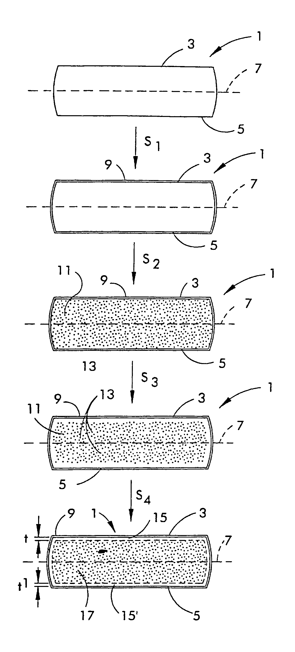
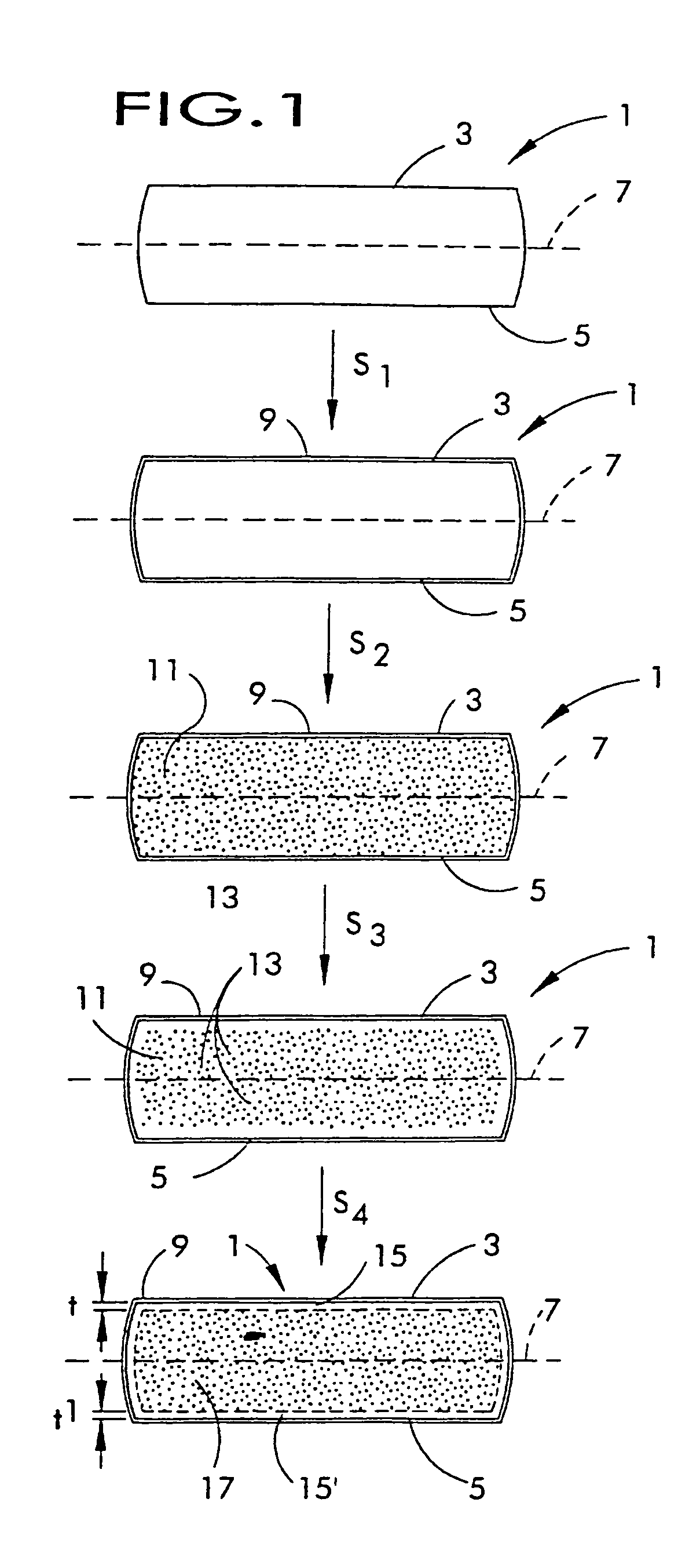
[0033]In another embodiment of the process of the present invention, the wafer 1 is heat-treated in an oxygen-containing atmosphere in step S1 to grow a superficial oxide layer 9 which envelopes wafer 1 prior to step S2. In general, the oxide layer will have a thickness which is greater than the native oxide layer which forms upon silicon (about 15 Å). In this second embodiment, the thickness of the oxide layer is typically at least about 20 Å. In some instances, the wafer will have an oxide layer that is at least about 25 or 30 Å thick. Experimental evidence obtained to-date, however, suggests that oxide layers having a thickness greater than about 30 Å, while not interfering with the desired effect, provide little or no additional benefit.

[0034]After forming the oxide layer, the rapid thermal annealing step is typically carried out in the presence of a nitriding atmosphere, that is, an atmosphere containing nitrogen gas (N2) or a nitrogen-containing compound gas such as ammonia wh...

fourth embodiment

[0041]In a fourth embodiment, therefore, the atmosphere during the rapid thermal annealing typically contains an oxygen partial pressure sufficient to obtain a denuded zone depth of less than about 30 microns. Typically the denuded zone depth ranges from greater than about 5 microns to less than about 30 microns, and can range from about 10 microns to about 25 microns, or from about 15 microns to about 20 microns. More specifically, the thermal treatment may be carried out in an atmosphere comprising a nitrogen-containing gas (e.g., N2), a non-oxygen, non-nitrogen containing gas (e.g., argon, helium, etc.), or a mixture thereof, and an oxygen-containing gas (e.g., O2 or pyrogenic steam), the atmosphere having an oxygen partial pressure sufficient to create an inward flux of interstitials (e.g., at least about 1 ppma, 5 ppma, 10 ppma or more) but less than about 500 ppma, preferably less than about 400 ppma, 300 ppma, 200 ppma, 150 ppma or even 100 ppma, and in some embodiments prefe...


PUM

PropertyMeasurementUnit
temperatureaaaaaaaaaa

Abstract

A process for imparting controlled oxygen precipitation behavior to a single crystal silicon wafer. Specifically, prior to formation of the oxygen precipitates, the wafer bulk comprises dopant stabilized oxygen precipitate nucleation centers. The dopant is selected from a group consisting of nitrogen and carbon, and the concentration of the dopant is sufficient to allow the oxygen precipitate nucleation centers to withstand thermal processing, such as an epitaxial deposition process, while maintaining the ability to dissolve any grown-in nucleation centers.

Description

CROSS-REFERENCE TO RELATED APPLICATION[0001]This application is a divisional application, and claims the benefit, of U.S. application Ser. No. 10 / 328,481, filed Dec. 23, 2002 now U.S. Pat. No. 6,808,781 which claims the benefit of Provisional Application 60 / 345,178, filed Dec. 21, 2001.BACKGROUND OF THE INVENTION[0002]The present invention generally relates to the preparation of semiconductor material substrates, especially silicon wafers, which are used in the manufacture of electronic components. More particularly, the present invention relates to a process for the treatment of silicon wafers which enables the wafers, during the heat treatment cycles of essentially any arbitrary electronic device manufacturing process to form an ideal, non-uniform depth distribution of oxygen precipitates.[0003]Single crystal silicon, which is the starting material for most processes for the fabrication of semiconductor electronic components, is commonly prepared with the so-called Czochralski pro...

Claims


Application Information

Patent Timeline
Patent Type & Authority Patents(United States)
IPC IPC(8): C30B15/20H01L21/322
CPCH01L21/3225H01L21/3226Y10T428/21
Inventor MULE'STAGNO, LUCIANOLIBBERT, JEFFREY L.PHILLIPS, RICHARD J.KULKARNI, MILINDBANAN, MOHSENBRUNKHORST, STEPHEN J.
Owner SUNEDISON SEMICON LIMITED UEN201334164H
Why Eureka
Try Eureka