

Photovoltaic cell including porous semiconductor layer, method of manufacturing the same and solar cell
a photovoltaic cell and semiconductor technology, applied in the field of photovoltaic cells including porous semiconductor layers, a manufacturing method of the same and a solar cell, can solve the problems of high cost for manufacturing silicon substrates, unsolved problems, and low yield, and achieve high yield, high yield, and high yield.
- Summary
- Abstract
- Description
- Claims
- Application Information
AI Technical Summary
Benefits of technology
Problems solved by technology
Method used
Image

Examples
example 1
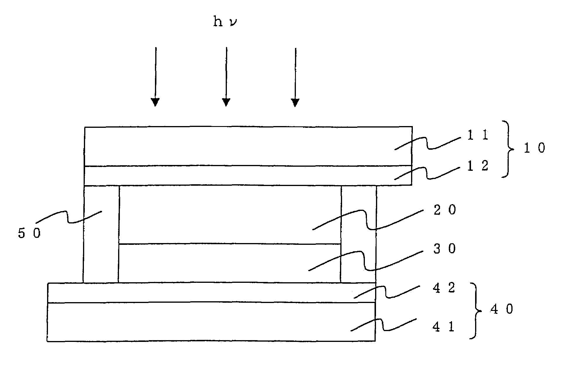
[0095]As shown in FIG. 1, a photovoltaic cell according to this example includes a porous semiconductor layer 20 formed on a conductive support 10, on which a photosensitive dye is adsorbed, a counter electrode support 40, a charge transport layer 30 filled between the porous semiconductor layer 20 and the counter electrode support 40 and a sealing material 50 sealing the sides thereof. The indication hv in FIG. 1 signifies light.
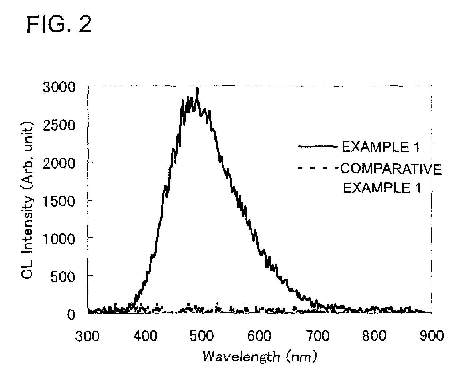
[0096]In this example, explanation is given of the case where the cathode luminescence property and the haze rate H of the porous semiconductor layer 20 are controlled. Also explained are experimental results in which improvement of the property was achieved by appropriately selecting a combination of a specific surface area S of the porous semiconductor layer, the haze rate H and surface density c.
[0097]The conductive support 10 was made of a glass substrate 11 on which a thin film of fluorine-doped tin oxide (SnO2:F) was formed by sputtering as a transpar...
example 2
[0111]A photovoltaic cell according to this example is the same as that of Example 1 except that the transparent electrode layer 12 (a thin film of SnO2:F) having a flat surface and the haze rate H of about 0 was replaced with a transparent electrode layer 12 (a thin film of SnO2:F) having a rough surface as shown in FIG. 7 and the haze rate H of about 0 to 30%. The roughness formed on the surface of the transparent conductive layer has Rmax of about 100 to 400 nm.
[0112]In this example, explanation is given of experimental results in which the property was improved by appropriately selecting a combination of the specific surface area S, the haze rate H and the surface density c of the porous semiconductor layer.
[0113]Other components than the transparent conductive layer 12 were formed in the same manner as Example 1 and hence detailed description thereof is omitted.
[0114]The transparent electrode layer 12 was formed in the following manner. First, in the same manner as in Example 1...
example 3
[0136]A photovoltaic cell according to this example includes, as shown in FIG. 14, a conductive support comprising a support 1 and a conductive film 2, a porous semiconductor layer 3 formed on the conductive support 1, on which a photosensitive dye is adsorbed, a counter electrode support comprising a support 5 and a conductive film 6 and an electrolyte layer filled as a charge transport layer 4 between the porous semiconductor layer 3 and the counter electrode support. The sides thereof are sealed with a sealing material 7.
[0137]First, on a glass substrate used as the translucent support 1, an SnO2 film was formed by sputtering as a translucent conductive film 2 of 0.1 μm thick.
[0138]Then, titanium oxide paste was coated on the conductive film 2, which was dried and baked to form a titanium oxide film (the porous semiconductor layer 3).
[0139]The titanium oxide paste was prepared as follows.
[0140]To 750 mL of 0.1 M nitric acid solution (manufactured by Kishida Chemical Co., Ltd.), 1...
PUM
 Abstract
Description
Claims
Application Information