

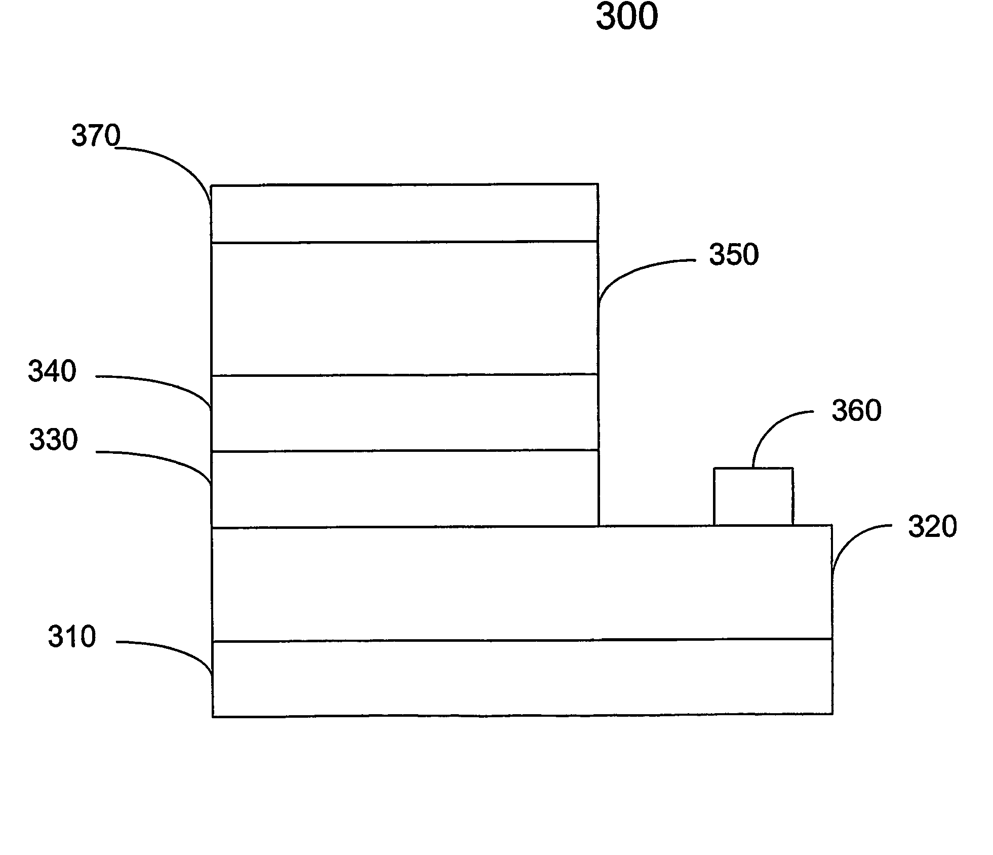
Semiconductor device with higher oxygen (02) concentration within window layers and method for making
a technology of semiconductor devices and window layers, applied in the direction of semiconductor devices, vacuum evaporation coatings, etc., can solve the problems of unable to give devices, low bandgap of approximately 2.42 ev, and failure to use materials with higher bandgap, etc., to achieve the effect of increasing the oxygen concentration of the deposited window layer, high efficiency pv, and increasing the oxygen concentration of the deposited layer
- Summary
- Abstract
- Description
- Claims
- Application Information
AI Technical Summary
Benefits of technology
Problems solved by technology
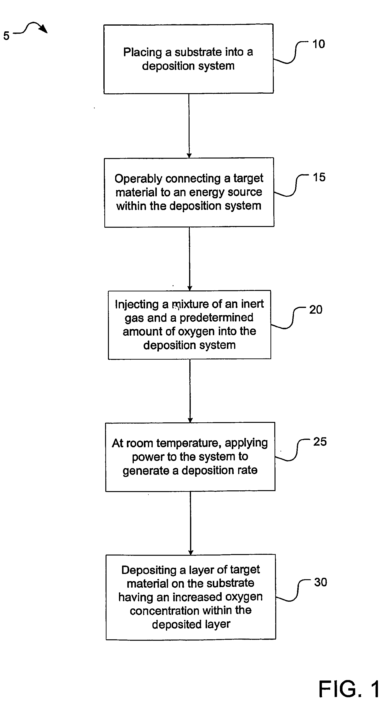
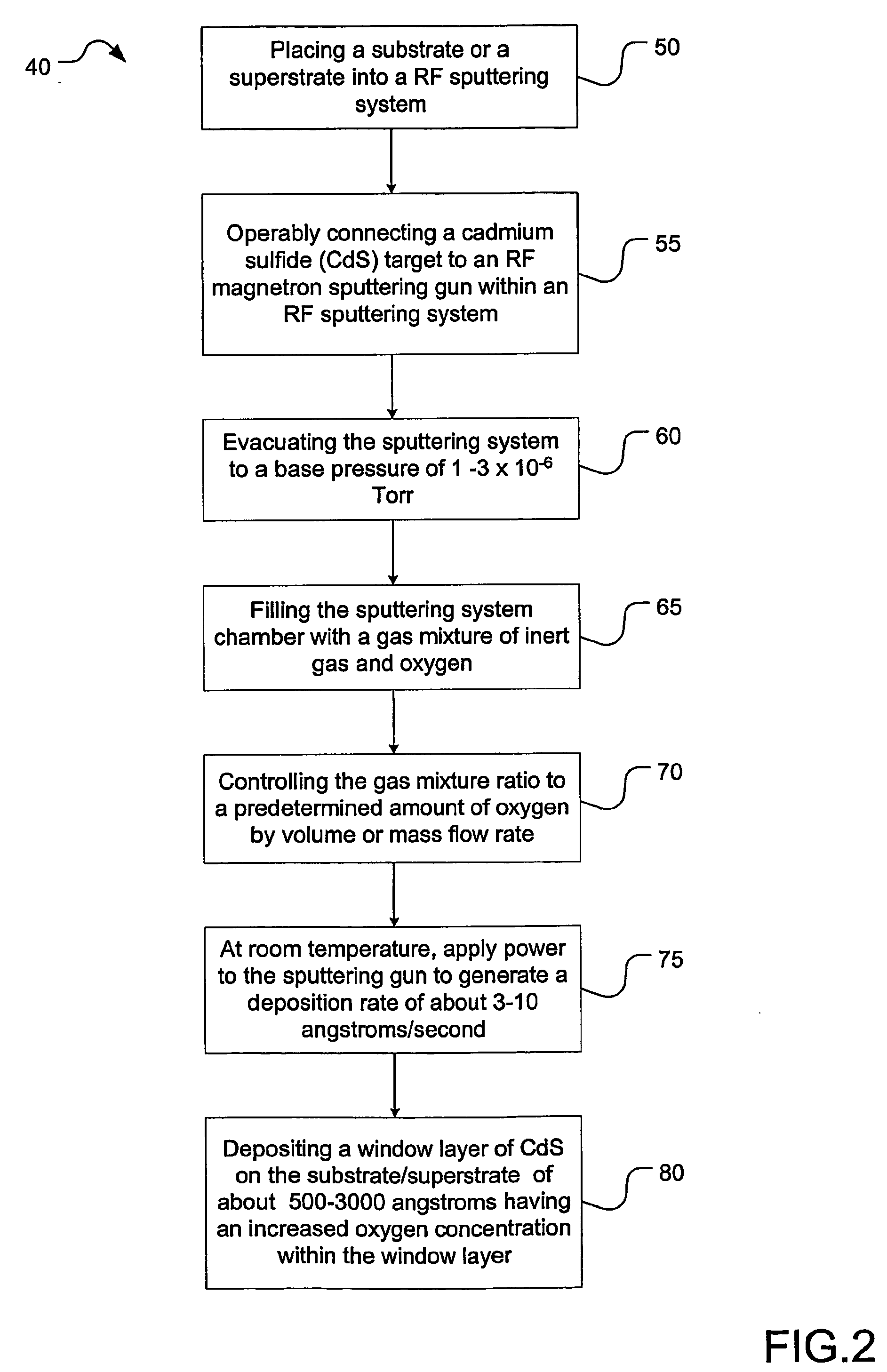
Method used
Image

Examples
Embodiment Construction
[0044] Definitions:
[0045] The following definitions are provided to facilitate understanding of certain terms used frequently herein and are not meant to limit the scope of the present disclosure:
[0046] The term “about” used herein refers to a tolerance of plus or minus ten percent (+ / −10%) of the value or quantity modified by the term.
[0047] Inert gas includes gases that lack reactivity, such as, but not limited to, stable gases such as noble gases and nitrogen (N2) and mixtures thereof, including inert nitrogen compounds.
[0048] Room temperature generally describes temperatures ranging from about twenty degrees Celsius (20° C.) to about thirty degrees Celsius (30° C.).
[0049] Atomic percent used herein is abbreviated as (at. %)
[0050] Photoconductivity (σL) is measured under illumination of 100 mW / cm2.
[0051] Dark photoconductivity (σD) is measured in the absence of light (in the dark).
[0052] Oxygen concentration within a deposited layer is measured by X-ray photoelectron spec...
PUM
| Property | Measurement | Unit |
|---|---|---|
| pressure | aaaaa | aaaaa |
| pressure | aaaaa | aaaaa |
| frequency | aaaaa | aaaaa |
Abstract
Description
Claims
Application Information