Silicon-based thin-film photoeclectric converter and method of manufacturing the same

a technology of photoelectric converters and thin films, which is applied in the manufacture of final products, basic electric elements, coatings, etc., can solve the problem that amorphous silicon cannot be used for a semiconductor device such as a photoelectric converter, and achieve the effects of reducing contact resistance at the interface, high hydrogen concentration, and resistivity reduction

Inactive Publication Date: 2009-05-28
KANEKA CORP
View PDF3 Cites 30 Cited by
  • Summary
  • Abstract
  • Description
  • Claims
  • Application Information

AI Technical Summary

Benefits of technology

[0024]The silicon-based thin-film photoelectric converter of the present invention includes: a substantially i-type photoelectric conversion layer of hydrogenated amorphous silicon or a hydrogenated amorphous silicon alloy; a substantially i-type buffer layer mainly made of hydrogenated amorphous silicon; and an n-type Si1-xOx layer (x is 0.25-0.6) stacked successively. The buffer layer has a high hydrogen concentration at its interface with the photoelectric conversion layer, and hence is in a state just before generation of silicon crystal phase parts, i.e., a state just before crystallization. Accordingly, reduction of resistivity and generation of the ...

Problems solved by technology

As is well known, since amorphous silicon containing no hydrogen includes defects caused by unpaired bonds (dangling bonds) at a...

Method used


Image

  • Silicon-based thin-film photoeclectric converter and method of manufacturing the same
  • Silicon-based thin-film photoeclectric converter and method of manufacturing the same
  • Silicon-based thin-film photoeclectric converter and method of manufacturing the same

Examples


example 1

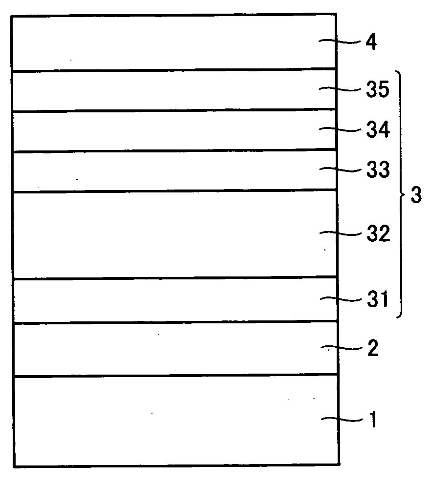
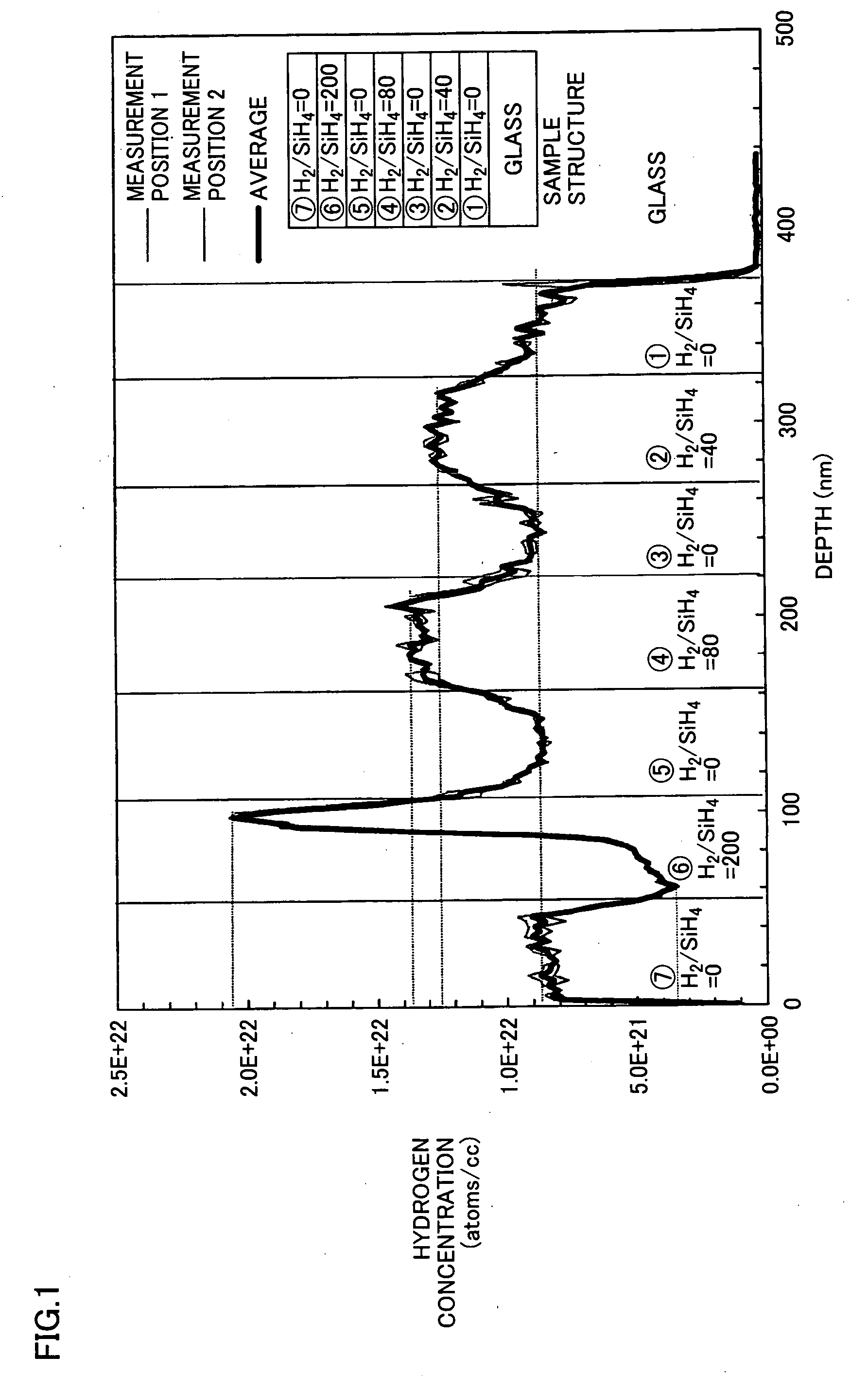
[0081]A single-junction amorphous photoelectric converter as shown in FIG. 4 was formed as Example 1. The device of Example 1 as shown in FIG. 4 differs from that of Comparative Example 2 in that substantially i-type buffer layer 33 mainly made of hydrogenated amorphous silicon was used instead of n-type microcrystalline silicon layer 37 in FIG. 7. Buffer layer 33 had a thickness of 5 nm. The deposition conditions for buffer layer 33 were as follows: chamber P5 serving as an n-type film-deposition chamber was used under conditions of an H2 / SiH4 flow ratio=80, a gas flow rate of H2 / SiH4=12800 / 160 sccm, a power supply frequency of 13.56 MHz, a power density of 100 mW / cm2, a pressure of 600 Pa, and a substrate temperature of 200° C. Hydrogen concentration at the buffer layer's interface with the photoelectric conversion layer was 1.37×10²² atoms / cc, when measured by SIMS. Hydrogen concentration of the photoelectric conversion layer was 8.5×10²² atoms / cc. In this case, tact time in cham...

example 2

[0084]A photoelectric converter having a structure similar to that of Example 1 was formed in Example 2, which was different from Example 1 only in that buffer layer 33 was deposited in chamber P4 serving as an i-type film-deposition chamber. Photoelectric conversion layer 32 was deposited in chamber P2, chamber P3, and chamber P4, and then buffer layer 33 was deposited within the remaining time allowed for chamber P4 and tact time in chamber P4 was 10 minutes. Furthermore, n-type Si1-xOx layer 34 and n-type microcrystalline silicon layer 35 were deposited in chamber P5, and tact time in chamber P5 was 11 minutes. Therefore, either of chambers P4 and P5 does not cause a rate-limiting factor in the manufacturing tact time, and hence manufacturing tact time in the CVD apparatus was 12 minutes, which was the same as that in Comparative Example 1.

[0085]As shown in Table 1, output properties of the photoelectric converter in Example 2 were as follows: Voc=0.883 V, Jsc=14.37 mA / cm2, FF=0....

example 3

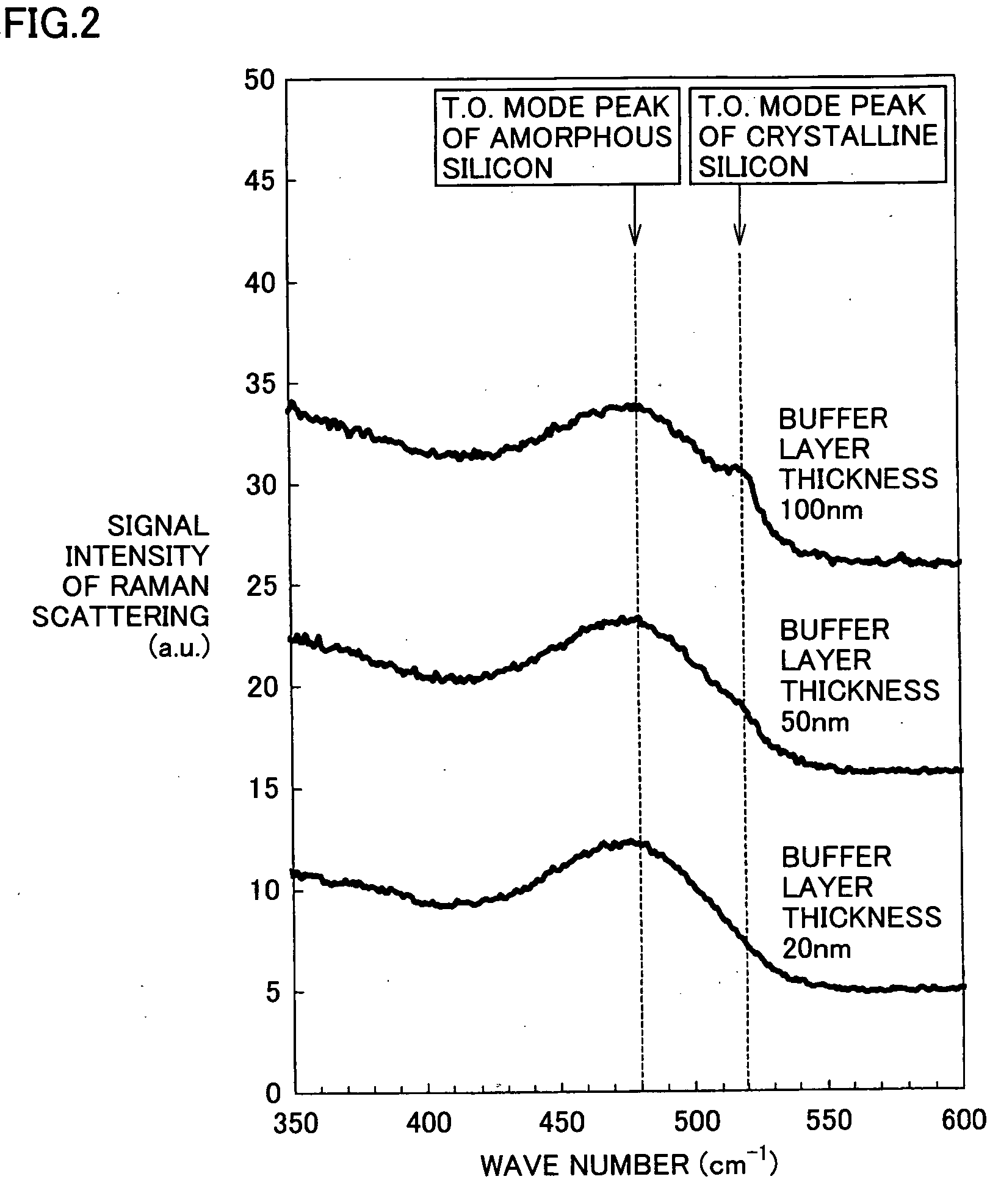
[0086]Photoelectric converters of Example 3 were formed with a similar structure and formation method as for the amorphous photoelectric converter of Example 1, except only that the thickness of buffer layer 33 was varied. At that time, the H2 / SiH4 for depositing the buffer layer was set to be 80. FIGS. 8-11 show correlation diagrams of various output properties of the photoelectric converters of Example 3 with respect to thickness of the buffer layer, by using relative values with respect to the output properties of the photoelectric converter of Comparative Example 2.

[0087]FIG. 8 is a correlation diagram that shows a relationship between thickness of the buffer layer and conversion efficiency (Eff) of the photoelectric converter in Example 3. As thickness of the buffer layer increases, Eff drastically increases to reach the maximum value at a thickness of 10-20 nm and then gradually decreases. The Eff becomes higher in the buffer layer's thickness range of 5 nm to 50 nm, as compar...


PUM


Abstract

In order to improve photoelectric conversion properties of a silicon-based thin-film photoelectric converter to which a conductive SiOx layer is inserted to obtain an optical confinement effect, the silicon-based thin-film photoelectric converter according to the present invention includes an i-type photoelectric conversion layer of hydrogenated amorphous silicon or an alloy thereof, an i-type buffer layer made of hydrogenated amorphous silicon, and an n-type Si1-xOx layer (x is 0.25-0.6) stacked successively, wherein the buffer layer has a higher hydrogen concentration at its interface with and as compared with the photoelectric conversion layer and has a thickness of at least 5 nm and at most 50 nm. Accordingly, generation of silicon crystal phase parts and reduction of resistivity are promoted in the n-type Si1-xOx layer, contact resistance at the interface is reduced, and FF of the photoelectric converter is improved, so that the photoelectric converter achieves improved properties.

Description

TECHNICAL FIELD[0001]The present invention relates to a silicon-based thin-film photoelectric converter that includes a substantially i-type photoelectric conversion layer of hydrogenated amorphous silicon or a hydrogenated amorphous silicon alloy and a conductive SiOx layer, and to a method of manufacturing the same. Incidentally, the terms “crystalline” and “microcrystalline” in the present specification are used even in the case of referring to a substance including partial amorphous phase parts, as used in the relevant technical field.BACKGROUND ART[0002]In recent years, attention has been focused on photoelectric converters that utilize the photoelectric effect in semiconductor to convert light into electric power, and they have been under intensive development. Among the photoelectric converters, a silicon-based thin-film photoelectric converter can be formed on a large-area substrate of glass or stainless steel at a relatively lower temperature, and hence cost reduction there...

Claims


Application Information

Patent Timeline
IPC IPC(8): H01L31/00B05D5/12H01L31/075
CPCH01L31/075Y02E10/548H01L31/202H01L31/076Y02P70/50
Inventor SASAKI, TOSHIAKIYAMAMOTO, KENJI
Owner KANEKA CORP
Why Eureka
Try Eureka