Semiconductor device fabrication method

a technology of semiconductor devices and fabrication methods, applied in semiconductor devices, semiconductor/solid-state device details, electrical apparatus, etc., can solve the problems of fluctuating characteristics of soi-cmos devices, and deteriorating performance of analog circuits

Inactive Publication Date: 2007-04-17
LAPIS SEMICON CO LTD
View PDF13 Cites 21 Cited by
  • Summary
  • Abstract
  • Description
  • Claims
  • Application Information

AI Technical Summary

Benefits of technology

[0020]An object of the invention is to provide a fabrication method for a semiconductor device and, more particularly, an SOI device, which forms an adequately activated substrate contact in the substrate contact region of a support substrate without substantially changing the conventional SOI-CMOS device formation process.
[0027]Further, ion implantation to form the substrate contact region is executed before providing a metal layer with a high melting point on the drain and source regions and siliciding the metal layer, and activation annealing of the substrate contact region can be performed simultaneously with the activation annealing of the drain and source regions. Accordingly, a low-resistance substrate contact can be formed.

Problems solved by technology

When CMOS technology is applied to high frequency circuits, in such cases the combined mounting of digital and analog circuits may be considered, the performance of the analog circuit is known to deteriorate due to crosstalk noise from the digital circuit.
This is because, when a noise enters the support substrate, there is a risk that characteristics of the SOI-CMOS device fluctuate under the influence of the noise and that the performance of the analog circuit deteriorates.
However, when annealing is performed at a temperature of 800° C. or more, adverse effects such as the aggregation of metal silicide formed as the drain electrode 286 and the source electrode 288 occur.
On the other hand, in order to activate the substrate contact region adequately and reduce the contact resistance, annealing at a temperature of 1000° C. or more is required, which means annealing at a temperature of 800° C. or less is inadequate.
As a result, a low contact resistance is not achieved.
Because the substrate contact hole must be formed deeply, the aspect ratio thereof becomes high and it is therefore sometimes impossible to perform adequate ion implantation in the substrate contact region.
As described above, the step to achieve the low contact resistance is complex in any conventional technology.

Method used


Image

  • Semiconductor device fabrication method
  • Semiconductor device fabrication method
  • Semiconductor device fabrication method

Examples


Embodiment Construction

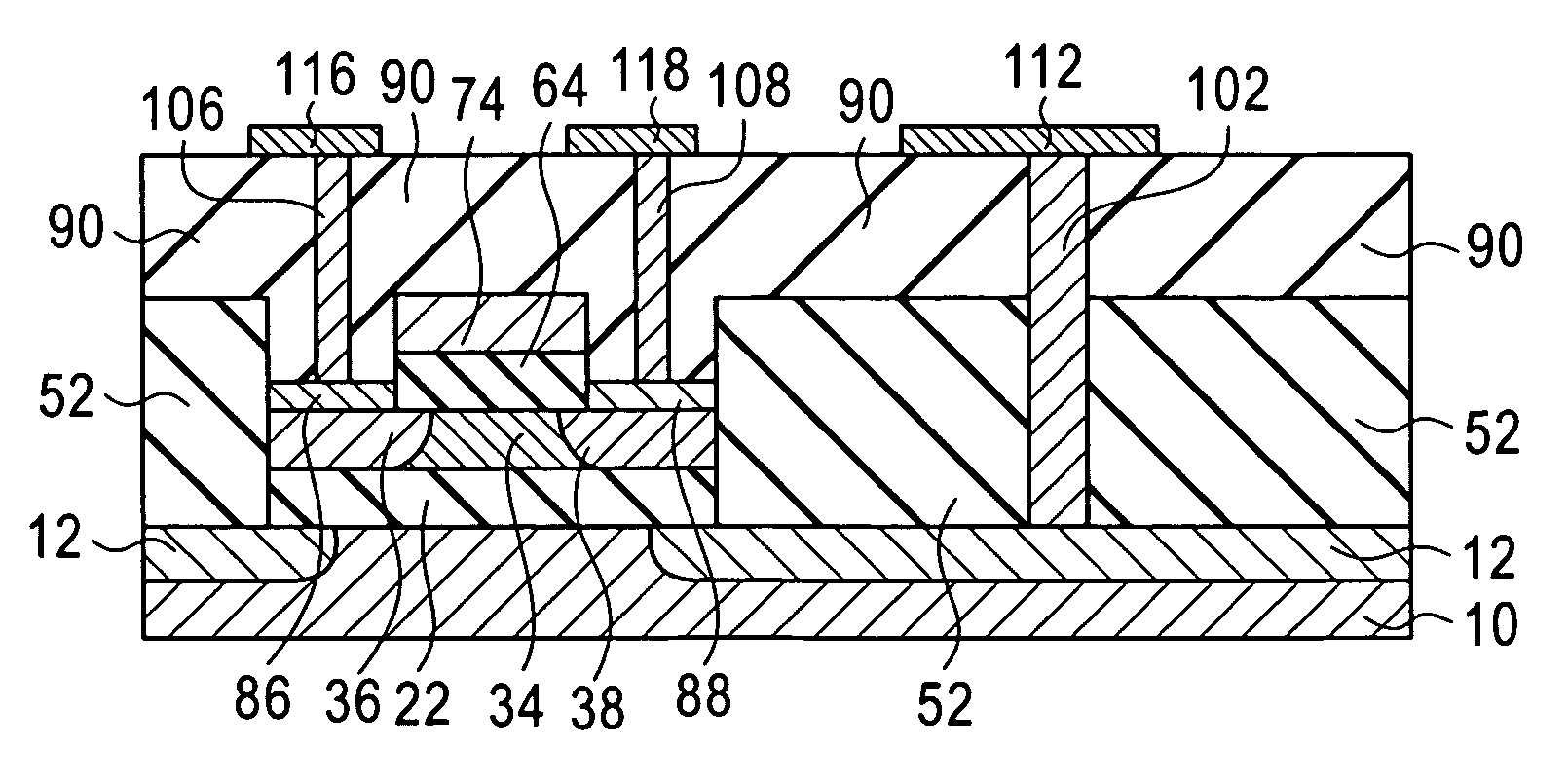
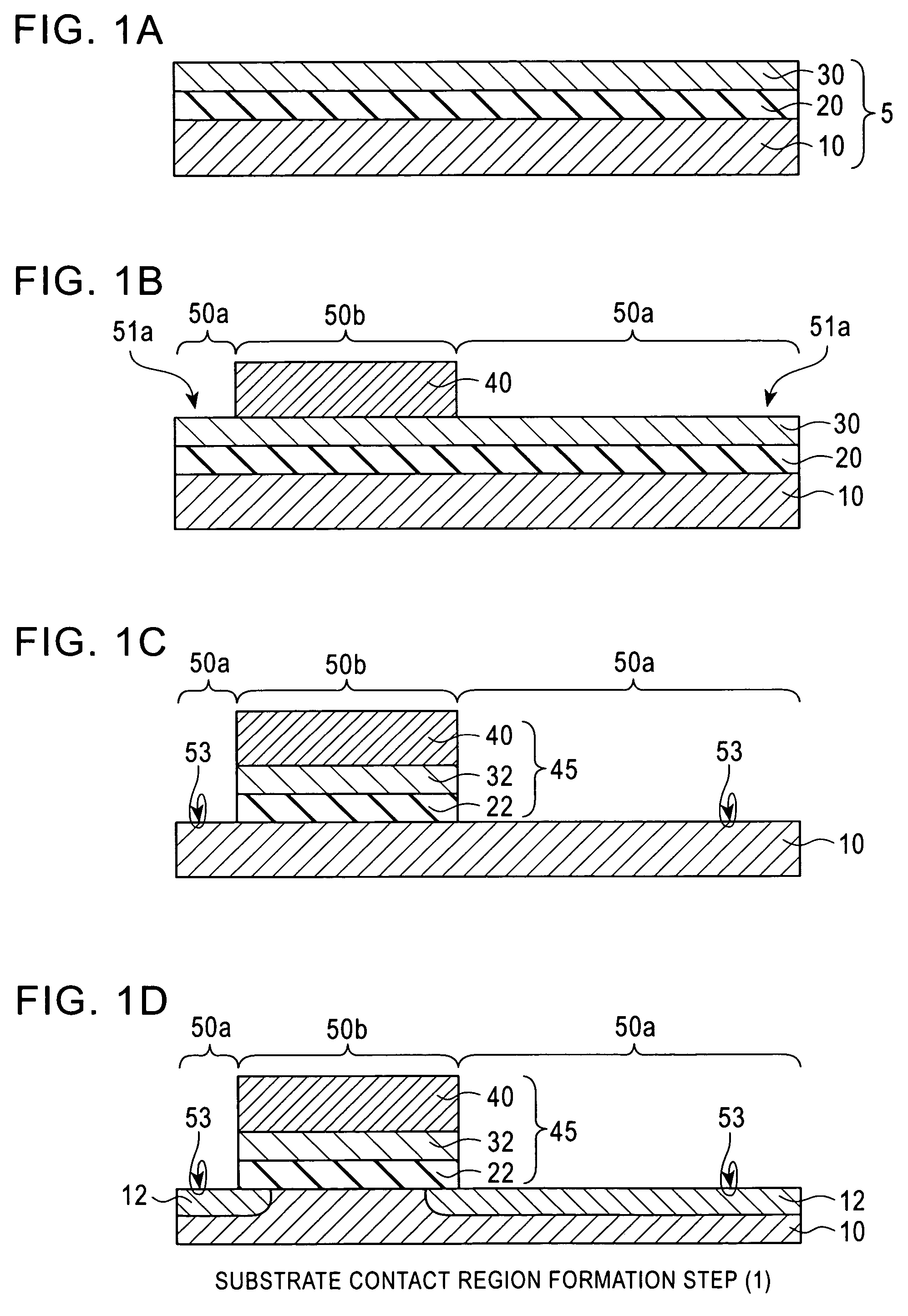
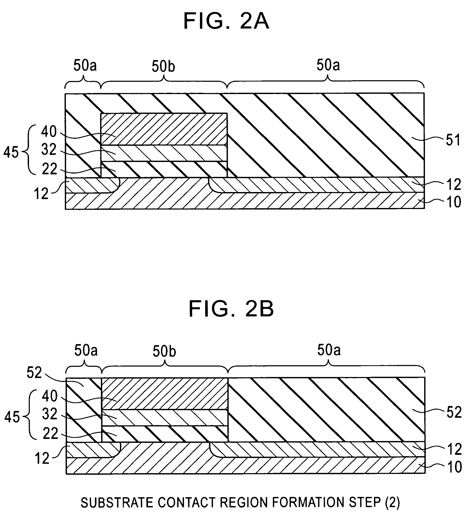
[0035]An embodiment of a semiconductor device fabrication method according to the invention will be described with reference to FIGS. 1A to 1D. It should be noted that the constitution and positional relationships of the embodiment are merely shown schematically to an extent necessary for an understanding of the invention. Further, although a preferred embodiment of the invention will be described hereinbelow, the composition (materials) of each constitution and the numerical conditions thereof and so forth are only preferred examples. Therefore, the invention is in no way limited to or by the following embodiment.

[0036]The semiconductor device fabrication method of the embodiment of the invention includes three steps, which are a substrate contact region formation step, a MOSFET formation step, and a contact formation step, as described hereinbelow. Each step includes a plurality of sub-steps.

[0037]The substrate contact region formation step will now be described with reference to ...


PUM


Abstract

The present invention adequately activates a substrate contact region of a support substrate without substantially changing the conventional SOI-CMOS device formation process. An exposed face of the support substrate is formed in an element isolation region of a layered substrate, which includes a support substrate having a first semiconductor layer, an insulating layer provided on the support substrate, and a second semiconductor layer provided on the insulating layer, by etching away the insulating layer and the second semiconductor layer. A substrate contact region is then formed in the support substrate by performing ion implantation from the side of the exposed face of the support substrate. Thereafter, an element isolation insulation layer is formed on the exposed face of the support substrate and a gate oxide film and a gate electrode are formed on the remaining second semiconductor layer. In addition, drain and source regions are formed by performing the ion implantation to the remaining second semiconductor layer with the gate electrode serving as a mask. Annealing to activate the substrate contact region, the drain region and the source region is then performed. Thereafter, a metal layer with a high melting point is formed on the drain and source regions and the metal layer is silicided through heat treatment.

Description

BACKGROUND OF THE INVENTION[0001]1. Field of the Invention[0002]The invention relates to a semiconductor device fabrication method and, more particularly, to a substrate contact formation method.[0003]2. Description of the Related Art[0004]Due to advances in CMOS technology of recent years, the functions of CMOS devices employing bulk Si substrates are improving rapidly. Therefore, applications of CMOS technology in higher frequency regions of the GHz band, which have been conventionally problematic, are becoming feasible. When CMOS technology is applied to high frequency circuits, in such cases the combined mounting of digital and analog circuits may be considered, the performance of the analog circuit is known to deteriorate due to crosstalk noise from the digital circuit.[0005]As compared with a CMOS device employing a bulk Si substrate, an SOI-CMOS device employs an SOI (Silicon On Insulator) substrate which has an insulating layer between a support substrate and an element regi...

Claims


Application Information

Patent Timeline
Patent Type & Authority Patents(United States)
IPC IPC(8): H01L21/8238H01L21/762H01L21/336H01L21/768H01L21/84H01L23/522H01L27/08H01L27/092H01L29/45H01L29/786
CPCH01L21/84H01L29/458H01L29/66772H01L29/78612H01L29/78648H01L2924/0002H01L2924/00
Inventor OKIHARA, MASAO
Owner LAPIS SEMICON CO LTD
Why Eureka
Try Eureka