PMOS transistor with compressive dielectric capping layer

a dielectric capping layer and transistor technology, applied in semiconductor devices, chemical vapor deposition coatings, coatings, etc., can solve the problem of film with relatively high compressive stress, and achieve the effect of enhancing the performance of the resulting transistor, preserving material quality, and ensuring the efficiency of the transistor fabrication process

Active Publication Date: 2007-05-08
NOVELLUS SYSTEMS
View PDF10 Cites 342 Cited by
  • Summary
  • Abstract
  • Description
  • Claims
  • Application Information

AI Technical Summary

Benefits of technology

[0009]The invention helps to solve some of the problems mentioned above by providing systems, structures and methods for generating compressive stress in the channel region of a PMOS transistor. Embodiments in accordance with the invention provide transistor architectures and fabrication processes for generating channel strain without adversely impacting the efficiency of the transistor fabrication process, while preserving the material quality an...

Problems solved by technology

Thus, ion bombardment arising from HFRF and LFRF energy during both depositi...

Method used


Image

  • PMOS transistor with compressive dielectric capping layer
  • PMOS transistor with compressive dielectric capping layer
  • PMOS transistor with compressive dielectric capping layer

Examples


example 1

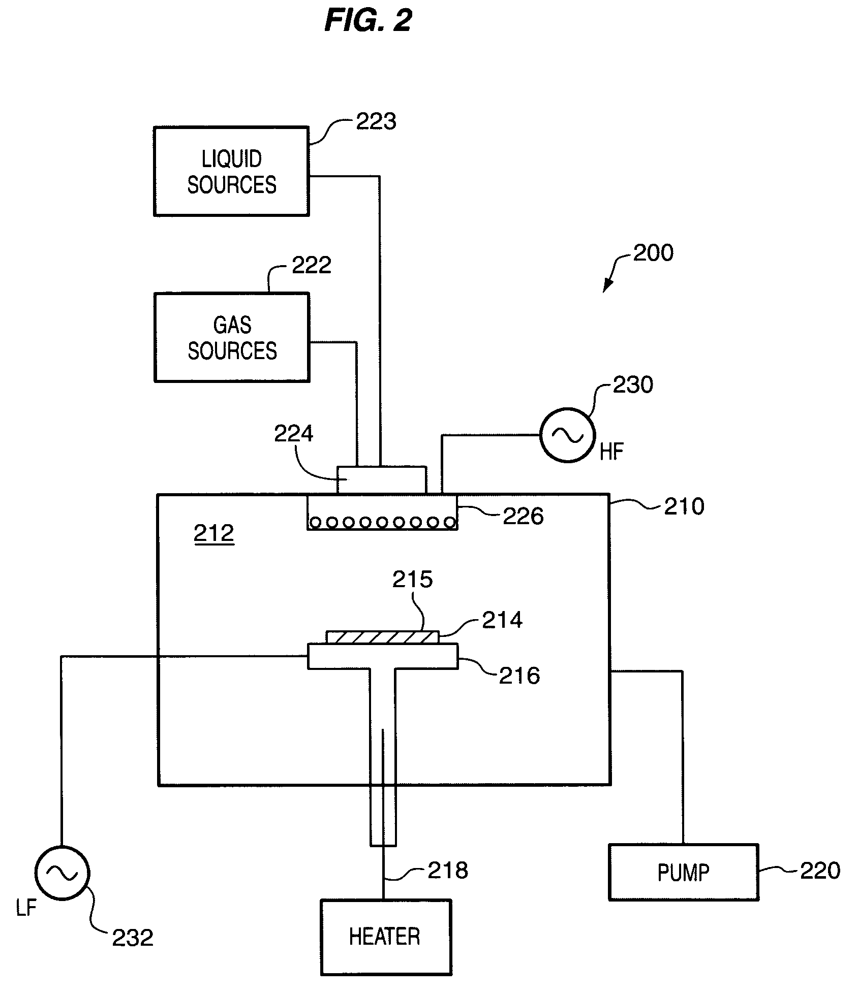
[0093]Silicon nitride (SiN) was deposited on the silicon substrate of a series of commercially-available 300 mm silicon semiconductor wafers. SiN was deposited on each wafer using a PECVD process in all four RF stations of a Novellus “Vector” apparatus. The deposition plasma conditions and the post-treatment plasma conditions were the same for all wafers, and are summarized here for the “Vector” apparatus as a whole. Flow rates and power values for each of the four RF stations correspond to one-fourth of the values listed below.

[0094]SiN Plasma Deposition Conditions:

[0095]

SiH4 flow: 600 sccmNH3 flow:1000 sccmN2 flow:35 liters / minHe gas flow: 6 liters / minHF-RF:300 W (13.6 MHz)LF RF:700 W (250 kHz)Pressure:2.1 TorrWafer temperature:400° C.

[0096]Post-Treatment Plasma Conditions:

[0097]

SiH4 flow:noneNH3 flow:1000 sccmN2 flow:35 liters / minHe gas flow: 6 liters / minHF-RF:300 W (13.6 MHz)LF RF:700 W (250 kHz)Pressure:2.1 TorrWafer temperature:400° C.

[0098]The distance between the showerhead ...

example 2

[0106]Silicon nitride (SiN) was deposited on the silicon substrate of a series of commercially-available 300 mm silicon semiconductor wafers. SiN was deposited on each wafer using a PECVD process in all four RF stations of a Novellus “Vector” apparatus. The deposition plasma conditions and the post-treatment plasma conditions were the same for all wafers, and are summarized here for each “Vector” RF station as a whole. Flow rates and power values for each of the four RF stations correspond to one-fourth of the values listed below.

[0107]SiN Plasma Deposition Conditions:

[0108]

SiH4 flow: 600 sccmNH3 flow:1000 sccmN2 flow:35 liters / minHF-RF:300 W (13.6 MHz)LF RF:700 W (250 kHz)Pressure:2.1 TorrWafer temperature:400° C.

[0109]Post-Treatment Plasma Conditions:

[0110]

SH4 flow:noneNH3 flow:1000 sccmN2 flow:35 liters / minHF-RF:300 W (13.6 MHz)LF RF:700 W (250 kHz)Pressure:2.1 TorrWafer temperature:400° C.

[0111]The distance between the showerhead gas inlet and the substrate surface was about 1.4...


PUM

PropertyMeasurementUnit
Timeaaaaaaaaaa
Timeaaaaaaaaaa
Thicknessaaaaaaaaaa

Abstract

A salicide layer is deposited on the source/drain regions of a PMOS transistor. A dielectric capping layer having residual compressive stress is formed on the salicide layer by depositing a plurality of PECVD dielectric sublayers and plasma-treating each sublayer. Compressive stress from the dielectric capping layer is uniaxially transferred to the PMOS channel through the source-drain regions to create compressive strain in the PMOS channel. To form a compressive dielectric layer, a deposition reactant mixture containing A1 atoms and A2 atoms is provided in a vacuum chamber. Element A2 is more electronegative than element A1, and A1 atoms have a positive oxidation state and A2 atoms have a negative oxidation state when A1 atoms are bonded with A2 atoms. A deposition plasma is generated by applying HF and LF radio-frequency power to the deposition reactant mixture, and a sublayer of compressive dielectric material is deposited. A post-treatment plasma is generated by applying HF and LF radio-frequency power to a post-treatment gas that does not contain at least one of A1 atoms and A2 atoms. Compressive stress in the dielectric sublayer is increased by treating the sublayer in the post-treatment plasma. Processes of depositing a dielectric sublayer and post-treating the sublayer in plasma are repeated until a desired thickness is achieved. The resulting dielectric layer has residual compressive stress.

Description

FIELD OF THE INVENTION[0001]The invention is related to the field of integrated circuit transistors, in particular to methods and structures for providing increased mobility of holes in PMOS transistors.BACKGROUND OF THE INVENTION[0002]As the design density of integrated circuits increases, and design features get smaller, there is a need for higher switching speeds in transistors.[0003]In un-strained silicon, the lowest energy level in the conduction band has six discrete electron states. Each state has a different momentum value, and only a small input of energy is required for an electron to move from one state to another. When the lattice is under tensile strain, its physical symmetry is broken, and with that the electronic symmetry. The lowest energy level of the conduction band is split, with two of the six original states dropping to a lower energy level and four rising to a higher energy level. Thus, it becomes more difficult for the electrons to be ‘scattered’ between the l...

Claims


Application Information

Patent Timeline
IPC IPC(8): H01L21/31
CPCC23C16/30C23C16/56H01L21/3105H01L21/3148H01L21/3185H01L29/665H01L29/7843H01L29/78H01L21/02274H01L21/02164H01L21/02205H01L21/02216H01L21/02112H01L21/022H01L21/02126H01L21/02211H01L21/0217H01L21/02167H01L21/0234
Inventor VARADARAJAN, BHADRI N.SIMS, JAMES S.SINGHAL, AKHIL
Owner NOVELLUS SYSTEMS
Why Eureka
Try Eureka