Solid electrolytic capacitor, stacked capacitor using the same, and fabrication method thereof

a solid electrolytic capacitor and aluminum technology, applied in the direction of electrolytic capacitors, liquid electrolytic capacitors, stacking capacitors, etc., can solve the problems of increasing capacity, reducing impedance, and increasing size, and it is difficult to obtain a capacitor having a sufficiently low impedance in a high frequency region, and achieves low impedance and small space. , the effect of large capacity

Inactive Publication Date: 2007-05-08
TOKIN CORP
View PDF4 Cites 12 Cited by
  • Summary
  • Abstract
  • Description
  • Claims
  • Application Information

AI Technical Summary

Problems solved by technology

Capacitors that are used in a high frequency region have conventionally been mainly multilayer ceramic capacitors which, however, cannot satisfy need for reduction in size, increase in capacity, and reduction in impedance.
Liquid or solid electrolyte used in those capacitors, for example, manganese dioxide, has a high resistivity value of 1 Ω·cm to 100 Ω·cm and therefore it has been difficult to obtain a capacitor having a sufficiently low impedance in a high frequency region.
As a result, there is a disadvantage in that the conductivity of the silver paste layer decreases to 1 / 10 to 1 / 100 of that of pure silver.
Further, as described above, since the aluminum foil at the anode portion is unsolderable, it is necessary to electrically connect a solderable metal of a different kind by the foregoing method or the like.
However, it has become difficult to achieve reduction in impedance by the use of the conventional silver paste or metal plate due to the influence of reduction in thickness and conductivity.
However, these methods each also generate an interfacial resistance in a pretreatment at the cathode portion, increase the thickness of a capacitor, and require more process steps and cost.

Method used


Image

  • Solid electrolytic capacitor, stacked capacitor using the same, and fabrication method thereof
  • Solid electrolytic capacitor, stacked capacitor using the same, and fabrication method thereof
  • Solid electrolytic capacitor, stacked capacitor using the same, and fabrication method thereof

Examples


example 1

[0049]In a basic element 20 shown in FIG. 5, a conductive polymer layer 3 in the form of a conductive polymer film is formed on a dielectric oxide film 2 of an aluminum foil 1 formed with the dielectric oxide film 2 by surface roughening. Symbol 11 denotes a resist for dividing into an anode portion and a cathode portion. In the basic element 20 after the formation of the conductive polymer film, a copper plating layer was directly formed as a first metal plating layer (I) 5a on the cathode portion conductive polymer layer 3 as shown in FIG. 3. Alternatively, after forming a graphite layer on the cathode portion conductive polymer layer 3, a copper plating layer was formed as a first metal plating layer (I) 5a. Then, the respective samples were each applied, as a pretreatment for anode portion copper plating, with a zincate treatment, with gold deposition, platinum deposition, or carbon deposition to form an anode deposition film 4, with masking so as not to form the oxide film at t...

example 2

[0052]As shown in FIG. 3, a first metal plating layer (I) 5a on polypyrrole and a second metal plating layer (II) 6a on a metal deposition layer 4 were formed by copper plating, respectively, according to the foregoing copper plating method and third metal plating layers (III) 7 were each formed by a copper-tin alloy plating layer, thereby preparing a solid electrolytic capacitor 101.

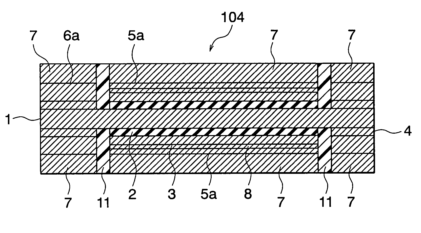
[0053]As shown in FIG. 4, a nickel plating layer was formed as a first layer 5a of a first metal plating layer (I) on a basic element 20 and a copper plating layer was formed as a second layer 5b on the first layer 5a, while, likewise, a nickel plating layer was formed as a first layer 6a of a second metal plating layer (II) and a copper plating layer was formed as a second layer 6b on the first layer 6a, and third metal plating layers (III) 7 were each formed by a copper-tin alloy plating layer, thereby preparing a solid electrolytic capacitor 102.

[0054]As shown in FIG. 6, a graphite layer 8 was formed...

example 3

[0057]After forming a plurality of solid electrolytic capacitors 101 on the frames shown in FIG. 8, the frames were stacked together and then copper-tin alloy plating layers 7 as third metal plating layers (III) 7 were heated and melted at 230° C. to 350° C. so as to be bonded together, thereby producing five-layer stacked capacitors 105 of this invention.

[0058]Further, the frames shown in FIG. 9 were stacked together at predetermined positions, then solid electrolytic capacitors 107 were joined together by the use of conductive paste and then cut at predetermined portions, thereby producing five-layer stacked capacitors 106.

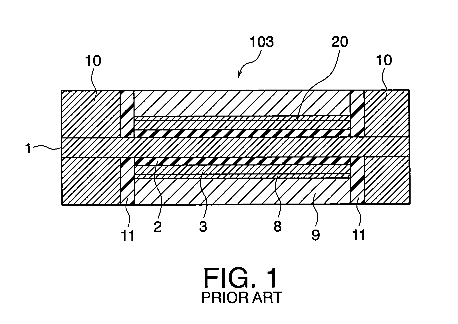
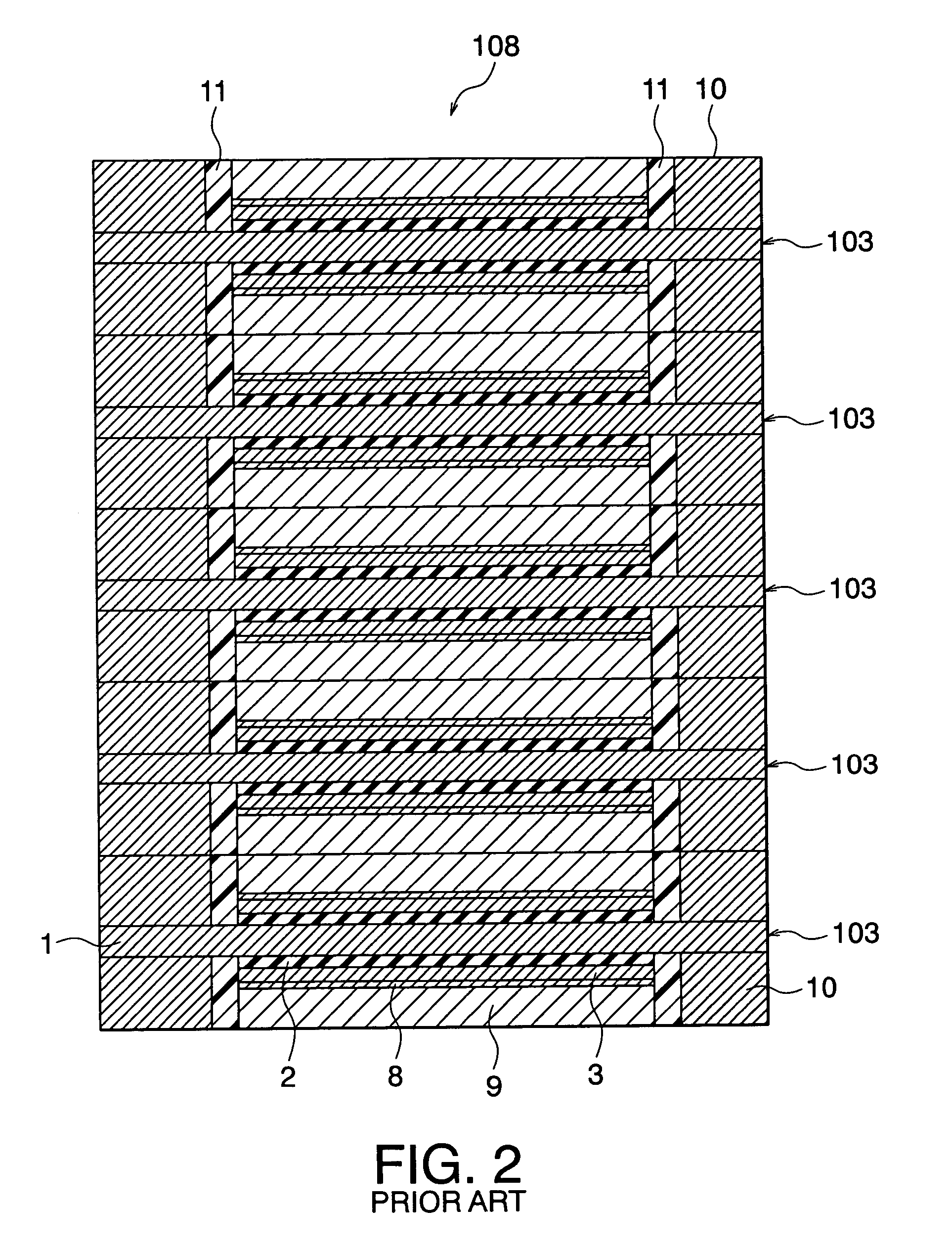
[0059]For comparison, there was produced a conventional five-layer stacked capacitor 108 using graphite, silver paste, and terminal plates as shown in FIG. 2.

[0060]FIG. 10 shows frequency-impedance characteristics of the stacked capacitors 105, 106, and 108, respectively.

[0061]As shown in FIG. 10, it is understood that the impedance of the stacked capacitor 105 ...


PUM

PropertyMeasurementUnit
melting pointaaaaaaaaaa
resistivityaaaaaaaaaa

Abstract

On a surface-roughened aluminum foil, an aluminum oxide film as an anodic oxide film is formed. Then, a conductive polymer layer as a solid electrolyte is formed thereon and thereafter a first metal plating layer is directly formed on the conductive polymer layer, thereby forming a cathode portion. On the other hand, a second metal plating layer is formed on another portion of the surface-roughened aluminum foil, which is not subjected to anodic oxidation or which is subjected to anodic oxidation followed by polishing or formation of an anode deposition film, to thereby form an anode portion. Third metal plating layers are formed at the anode and the cathode portions to obtain a capacitor element. A plurality of capacitor elements are stacked and bonded together by fusion after formation of the third metal plating layers. Alternatively, the capacitor elements may be bonded together by a conductive paste without the third metal layers.

Description

[0001]This application claims priority to prior Japanese patent application JP 2004-214344, the disclosure of which is incorporated herein by reference.BACKGROUND OF THE INVENTION[0002]This invention relates to a thin-type aluminum solid electrolytic capacitor using a single-plate aluminum foil and, more specifically, relates to a capacitor fabrication method that directly forms a metal plating layer without a pretreatment at a cathode portion and-then forms a metal plating layer at an anode portion to thereby realize low impedance characteristics at high frequencies and achieve an increase in capacity with stacked layers.[0003]In recent years, following miniaturization, speed-up, and digitization of electronic devices, there has been a strong demand for small-size, large-capacity, and low-impedance capacitors having excellent high-frequency characteristics also in the field of capacitors.[0004]Capacitors that are used in a high frequency region have conventionally been mainly multi...

Claims


Application Information

Patent Timeline
Patent Type & Authority Patents(United States)
IPC IPC(8): H01G9/04H01G9/145
CPCH01G9/012H01G9/0425H01G9/045H01G9/15H01G4/30H01G11/48H01G9/26Y10T29/417Y02E60/13
Inventor SAITO, TAKESHITOITA, SADAMUYOSHIDA, KATSUHIRO
Owner TOKIN CORP
Why Eureka
Try Eureka