
Wire grid polarizer and method for producing same

a polarizer and wire grid technology, applied in the direction of polarising elements, instruments, other domestic objects, etc., can solve the problems of low light transmittance and quenching ratio, increased cost, and difficulty in producing polarizers using polar cores, etc., to achieve high quenching ratio, high transmittance, and high degree of polarization

Active Publication Date: 2007-05-22
ENPLAS CORP
View PDF5 Cites 44 Cited by
  • Summary
  • Abstract
  • Description
  • Claims
  • Application Information

AI Technical Summary

Benefits of technology

The present invention provides a thin wire grid polarizer with high transmittance, quenching ratio, and degree of polarization, and a method for producing it at low costs. The wire grid polarizer comprises a light transmissible substrate, a thin film layer of a light transmissible hydrophilic resin, and a plurality of metal fine wires formed on the thin film layer. The wire grid polarizer may further comprise a protective layer of a light transmissible hydrophobic resin. The method for producing the wire grid polarizer involves forming an underlayer on a substrate, forming a thin film layer of a hydrophobic resin on the underlayer, preparing a die with plurality of protrusions, pressing the protrusions of the die onto the thin film layer of the hydrophobic resin to form metal fine wire forming grooves, and forming each metal fine wire in a corresponding metal fine wire forming groove. The substrate may have a light transmissible mold releasing layer for easy removal of the substrate after the metal fine wires are formed. The underlayer may be a metal thin film or a thin film of a light transmissible hydrophilic resin.

Problems solved by technology

However, there are problems in that the heat resistance, moisture resistance and chemical resistance of the polarizer disclosed in Japanese Patent Laid-Open No. 2003-43257 are low, and that the light transmittance and quenching ratio as optical characteristics thereof are also low, although there is an advantage in that it can be produced in large quantities at low costs, since it is produced by using a high polymer film.
However, it is not easy to produce the polarizer using the polar core and the polarizer disclosed in Japanese Patent Laid-Open No. 5-208844.
In this case, since it is required to carry out reduction and deposition in a specific gas at a high temperature, there is a problem in that it is required to use a special equipment for carrying out such processes, so that costs are increased.
In addition, it is required to carry out heating and extension or orientation, so that it is difficult to produce a large-area polarizer at a time.
However, in a method for producing the wire grid polarizer disclosed in Japanese Patent Laid-Open No. 10-153706, the electron beam (EB) lithography system is unsuitable for the writing in a wide area, since the writing area at a time is small and since it takes a lot of writing time.
The X-ray lithography is not a desired method in view of mass productivity and production costs in the present circumstances, since the X-ray lithography system is very expensive and uses a very expensive photomask.
In addition, in the method for producing the wire grid polarizer, part of metal pieces lifted off are residual to cause the deterioration of characteristics, and if an expensive noble metal is used, most of metal portions lifted off are useless materials, so that costs are increased.
However, it is difficult to work a very fine polarizer required as the above described polarizer.
However, there is a problem in that these systems are very expensive in comparison with the i-line stepper which is a conventional exposure system.
However, even if the nano-imprint lithography method is used, a problem remains when metal wires having a size of 100 nm or less are precisely and repeatably formed in a large area.

Method used


Image

  • Wire grid polarizer and method for producing same
  • Wire grid polarizer and method for producing same
  • Wire grid polarizer and method for producing same

Examples


Embodiment Construction

[0049]Referring now to the accompanying drawings, the preferred embodiments of a wire grid polarizer and a method for producing the same according to the present invention will be described below in detail.

[0050]In a preferred embodiment of the present invention, in order to form metal fine wires of a very fine metal pattern, a pattern having a very fine period structure (a structure that protrusions are arranged in parallel at a very fine period), which is formed on the surface of a die, is transferred by the nano-imprint lithography technique.

[0051]The die will be briefly described below. The die is mainly made of silicon (Si) or quartz. The die may be produced by the following procedures.

[0052]First, a metal thin film having a predetermined thickness is deposited on a substrate of Si or quarts by a technique, such as sputtering. Then, a resist (an electron beam resist) is applied on the metal thin film. The resist is exposed to electron beams by the electron beam (EB) lithography...


PUM

PropertyMeasurementUnit
wavelength bandaaaaaaaaaa

Abstract

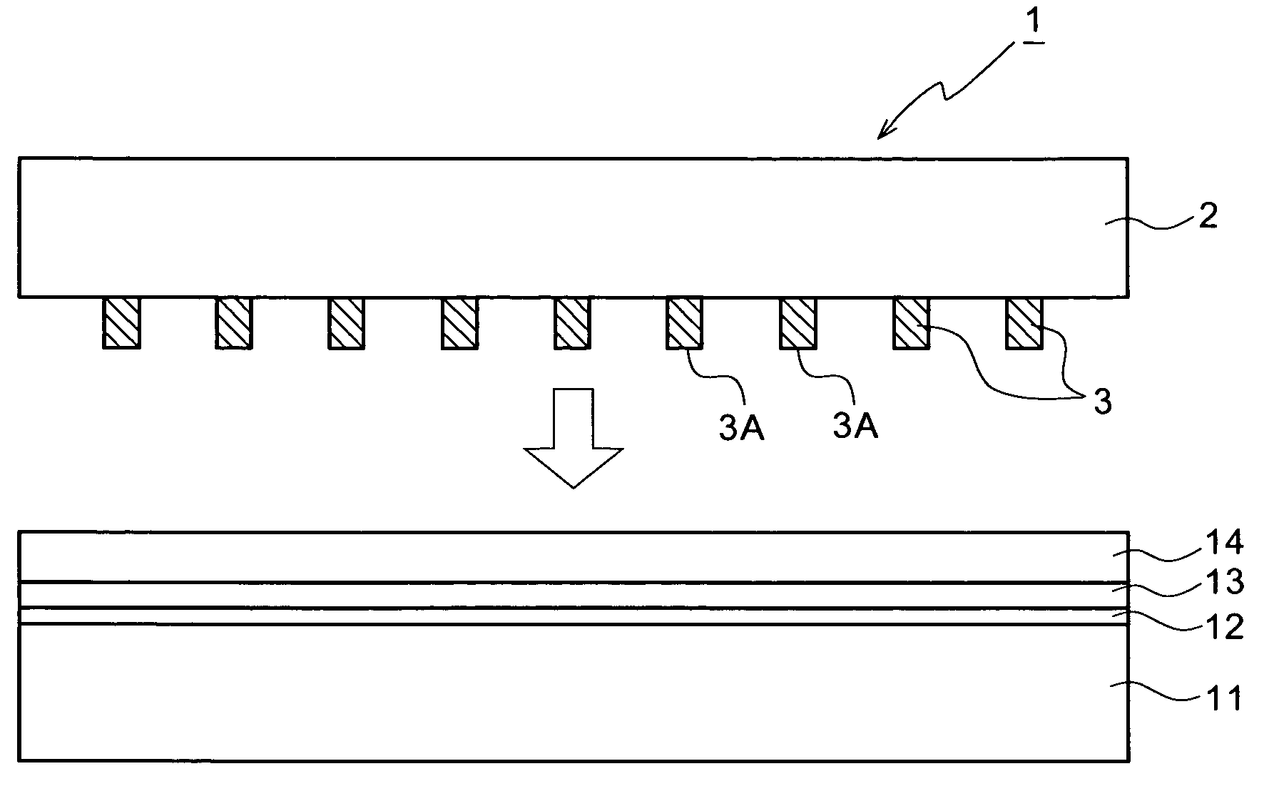
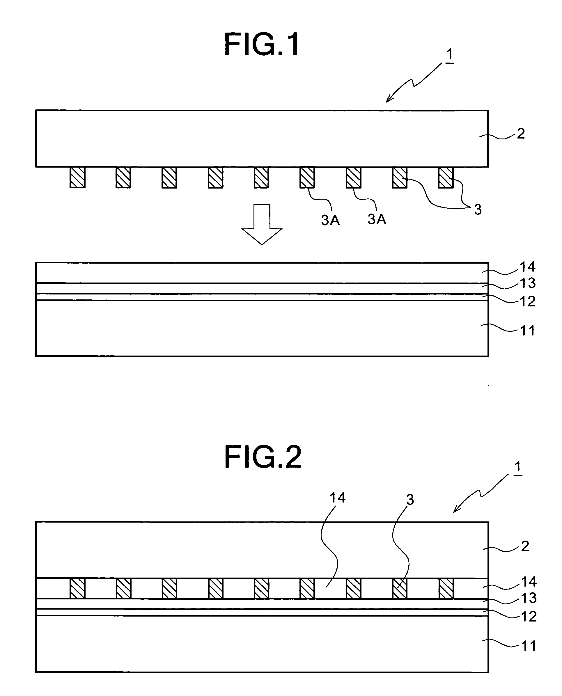
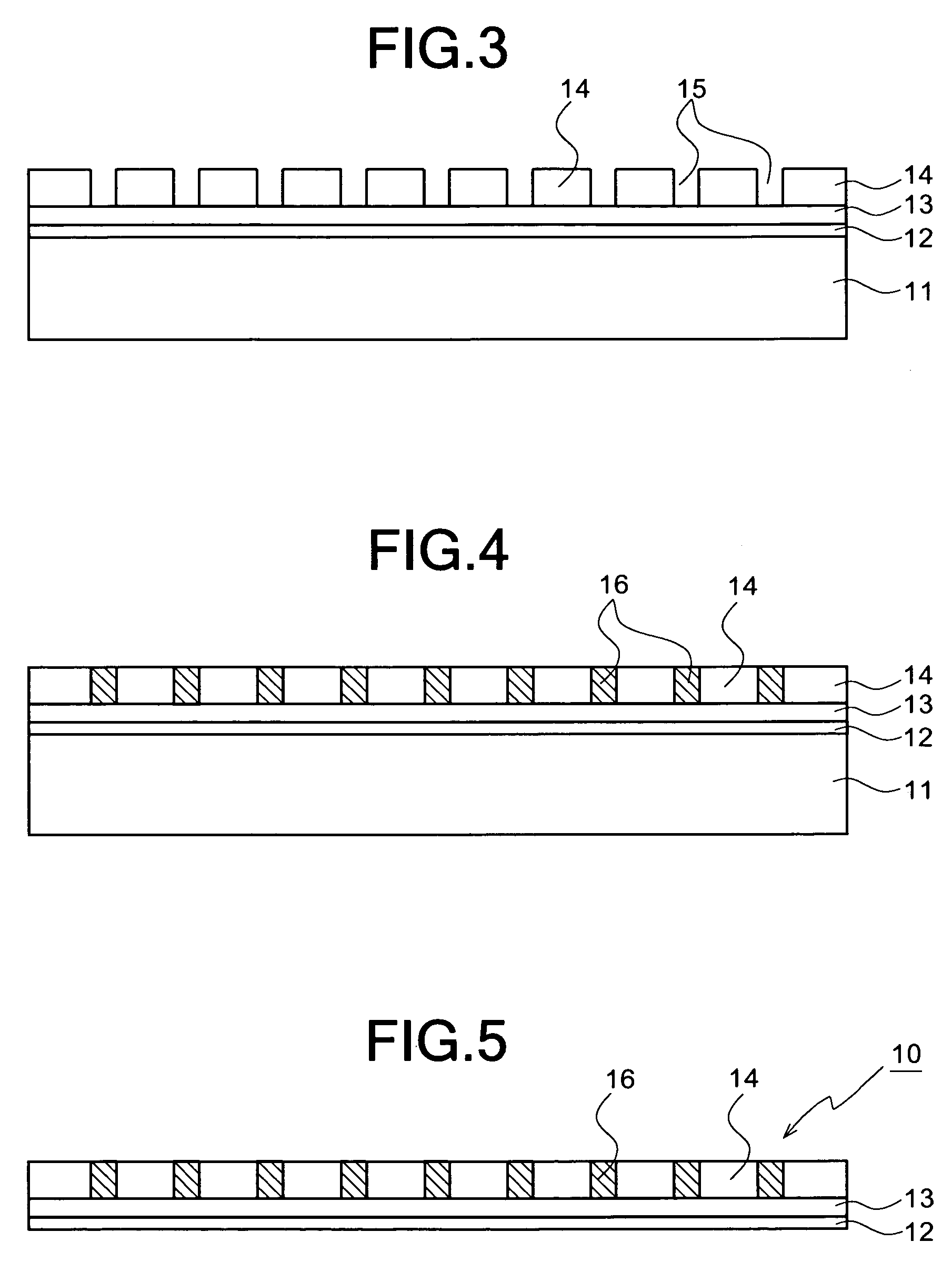
There are provided a thin wire grid polarizer having a high transmittance, a high quenching ratio and a high degree of polarization, and a method for producing the same at low costs. A fluoridated polyimide thin film 12, a hydrophilic thin film 13 and a hydrophobic thin film 14 are sequentially stacked on a glass substrate 11 to be pressed by a die 1 from the side of the hydrophobic thin film 14 to transfer the fine pattern of groove forming protrusions 3 of the die 1 to the hydrophobic thin film 14 and hydrophilic thin film 13 by the nano-imprinted lithography technique, and then, metal fine wires are caused to grow by plating.

Description

BACKGROUND OF THE INVENTION[0001]1. Field of the Invention[0002]The present invention generally relates to a wire grid polarizer and a method for producing the same. More specifically, the invention relates to a wire grid polarizer which is used for optical communication, optical recording, display or the like, and a method for producing the same.[0003]2. Description of the Prior Art[0004]As an example of a polarizer, there is widely known a polarizer utilizing optical anisotropy which is obtained by extending or orienting a high polymer film (see, e.g., Japanese Patent Laid-Open No. 2003-43257). Such a polarizer of a high polymer film is mainly used for a display, such as a liquid crystal panel. However, there are problems in that the heat resistance, moisture resistance and chemical resistance of the polarizer disclosed in Japanese Patent Laid-Open No. 2003-43257 are low, and that the light transmittance and quenching ratio as optical characteristics thereof are also low, although...

Claims


Application Information

Patent Timeline
Patent Type & Authority Patents(United States)
IPC IPC(8): B29D11/00G02B5/30
CPCG02B5/3058
Inventor SUGANUMA, TAKAYOSHI
Owner ENPLAS CORP
Learn More