High dielectric constant composite material and multilayer wiring board using the same

a composite material and high dielectric constant technology, applied in the direction of combination recording, conductive materials, record information storage, etc., can solve the problems of low heat resistance of organic substrates, inability to directly apply conventional coating and sintering techniques using metal or insulators, such as those practiced with ceramic substrates, and the difficulty of handling them. , to achieve the effect of low dielectric loss tangent and high dielectric constan

Inactive Publication Date: 2007-05-22
HITACHI LTD
View PDF10 Cites 9 Cited by
  • Summary
  • Abstract
  • Description
  • Claims
  • Application Information

AI Technical Summary

Benefits of technology

[0007]An object of the present invention is to provide a high dielectric constant composite material having a volume resistivity of 109 Ω or higher and also maintaining a high dielectric constant of 15 or above and a low dielectric loss tangent of 0.1 or below even in the high frequency region of several tens GHz order, and a multilayer wiring board using such a composite material.
[0008]Another object of the present invention is to provide a high dielectric constant composite material compounded with an organic resin capable of forming a passive element directly on a surface or interior of a printed wiring board, and good in processability, and a multilayer printed wiring board using the same.

Problems solved by technology

On the other hand, with the progress of miniaturization of the passive elements, there arose a problem in that their handling became more difficult in the manufacture and packaging thereof, and the limitation of the conventional technology in this line has become apparent.
The conventional coating and sintering techniques using a paste of a metal or an insulator, such as practiced with the ceramic substrates, can not be directly applied to the other types of substrates, especially organic substrates which are low in heat resistance.
High loading of an inorganic filler in a resin, however, tends to cause formation of voids when the resin is cured, due to bad compatibility of inorganic fillers with resins.
Further, because of low interfacial adhesion between inorganic filler and resin, there tends to take place separation at the interface.
Therefore, use of a resin composite with high inorganic filler loading as an insulating material raises the concern that reliability be lowered in relation to dielectric strength or leakage current.
Also, the method using ECR-CVD has problems in that a specific apparatus must be used, that it is impossible to form the dielectric films at low cost by a batch process, and that it is difficult to form a dielectric film having a complicate configuration.
Although such a composite material shows a satisfactory dielectric constant of not less than several ten, it suffers a dielectric loss tangent of not smaller than 0.1 due to skin effect, and more seriously, such an organic resin / metal composite is very low in insulating performance.
Further, miscibility of organic resin with metal is bad like inorganic materials.

Method used


Image

  • High dielectric constant composite material and multilayer wiring board using the same
  • High dielectric constant composite material and multilayer wiring board using the same
  • High dielectric constant composite material and multilayer wiring board using the same

Examples


example 1

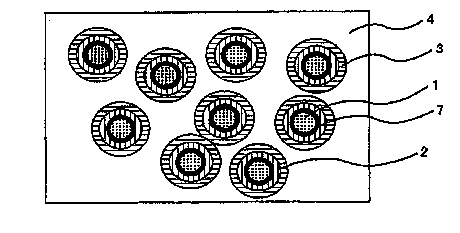
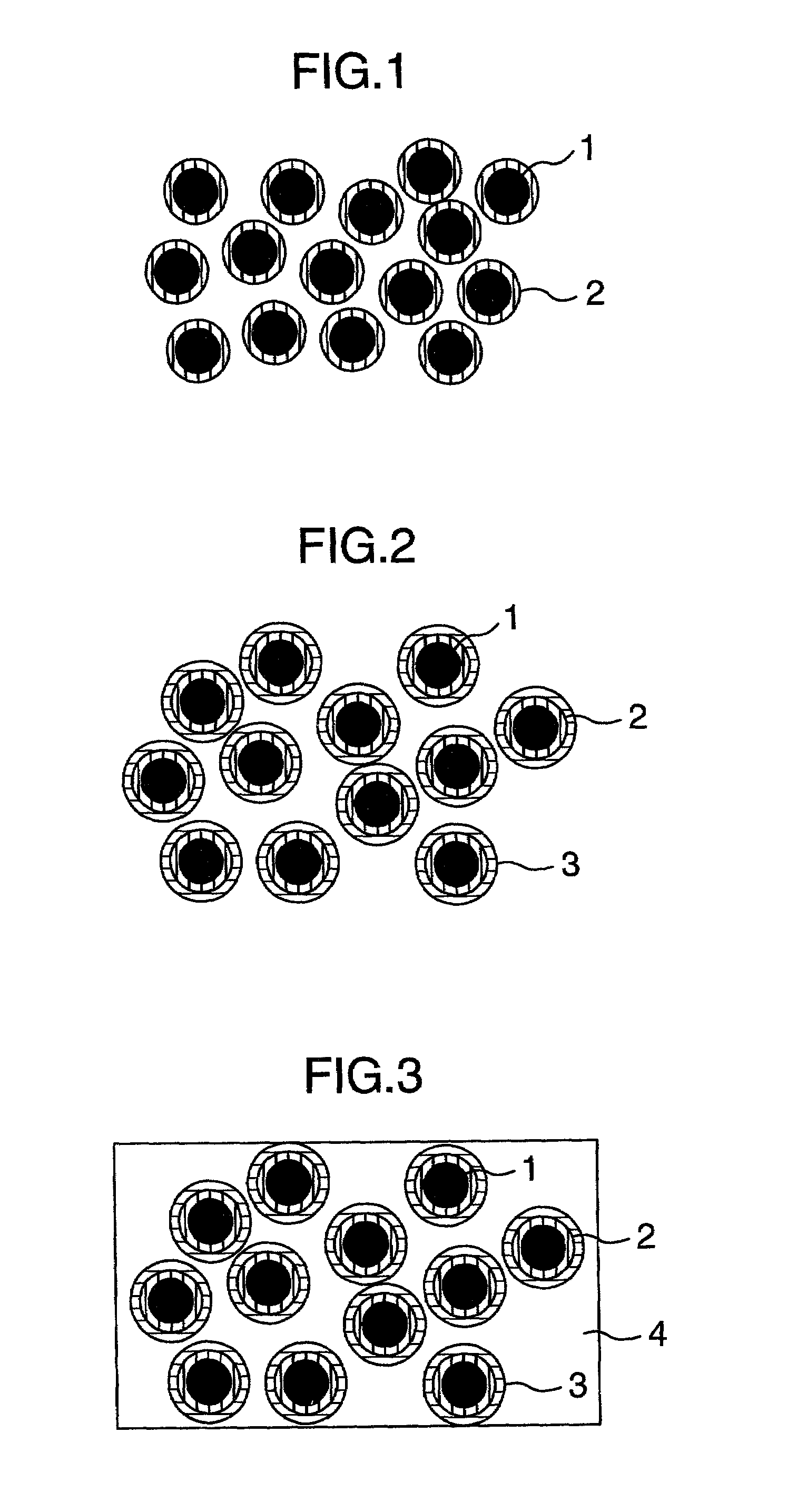
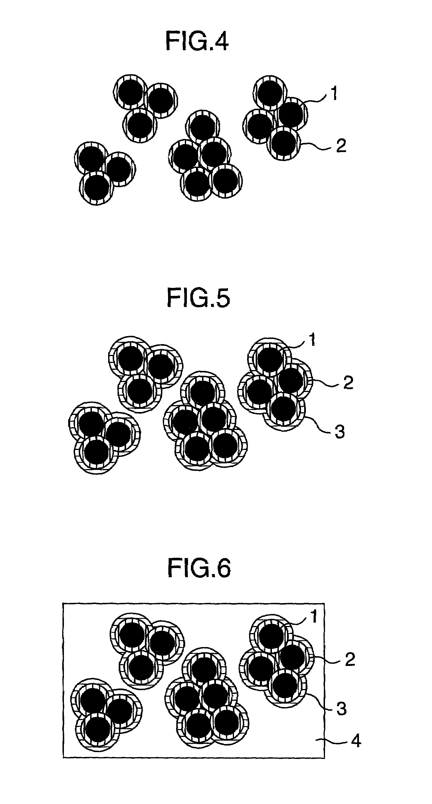
[0046]A process for producing a high dielectric constant composite material according to the first embodiment of the present invention is explained below. In this Example, EP828 (produced by Yuka Shell Epoxy Co., Ltd.) was used as epoxy resin, m-phenylenediamine (produced by Wako Pure Chemical Industries, Ltd.) as epoxy resin curing agent, and 2E4MZ-CN (produced by Shikoku Chemicals Corp.) as curing accelerator. Iron powder having an average particle size of 0.5 μm was used as a starting material for the high dielectric constant composite material. For the insulation of iron powder, a phosphate-based chemical treating solution containing 0.4 mol / l of benzotriazole as rust inhibitor and 0.1% by weight of EF104 (produced by Tohchem Products Corp.) as surfactant was used. S510 (produced by Chisso Corp.) was used as surface treating solution for the insulated iron powder.[0047](1) To 1 kg of iron powder having an average particle size of 0.5 μm, 200 ml of the insulating treatment soluti...

example 2

[0054]A process for producing the high dielectric composite material according to the second embodiment of the present invention is explained below. In this Example, EP1001 (produced by Yuka Shell Epoxy Co., Ltd.) was used as epoxy resin, dicyandiamide (produced by Wako Pure Chemical Industries, Ltd.) as epoxy resin curing agent, and 2E4MZ-CN (produced by Shikoku Chemicals Corp.) as curing accelerator. Zinc powder having as average particle size of 0.5 μm was used as high dielectric constant material. For the insulation of zinc powder, a phosphate-based chemical treating solution comprising 0.4 mol / l of benzotriazole as rust inhibitor and 0.1% by weight of EF104 (produced by Tohchem Products Corp.) as surfactant was used. S510 (produced by Chisso Corp.) was used as surface treating solution for iron powder after the insulation treatment.[0055](1) To 1 kg of zinc powder having an average particle size of 0.5 μm, 200 ml of the insulation treating solution was added and the mixture was...

example 3

[0061]A process for producing the high dielectric constant composite material according to the third embodiment of the present invention is explained below. In this Example, EP806 (produced by Yuka Shell Epoxy Co., Ltd.) was used as epoxy resin, m-phenylenediamine (produced by Wako Pure Chemical Industries, Ltd.) as epoxy resin curing agent, and 2E4MZ-CN (produced by Shikoku Chemicals Corp.) as curing accelerator. A zinc powder having an average particle size of 3 μm was used as a starting material for the high dielectric constant composite material. For the insulation of the zinc powder, a phosphate-based chemical treating solution containing 0.4 mol / l. of benzotriazole as rust inhibitor and 0.1% by weight of EF104 (produced by Tohchem Products Corp.) as a surfactant was used. S510 (produced by Chisso Corp.) was used as a surface treating solution for the insulated zinc powder.[0062](1) To 1 kg of zinc powder having an average particle size of 3 μm, 200 ml of the insulating treatme...


PUM

PropertyMeasurementUnit
dielectric constantaaaaaaaaaa
agglomerate sizeaaaaaaaaaa
particle sizeaaaaaaaaaa

Abstract

A high dielectric composite material obtained by subjecting submicron particles of an inorganic filler containing a metal as its essential component to an insulating treatment such as a chemical treatment, further subjecting to a surface treatment for improving their compatibility with organic resins, and then dispersing in an organic resin, has a dielectric constant of 15 or above, with its dielectric loss tangent in the frequency region of from 100 MHz to 80 GHz being 0.1 or less, and can therefore be used effectively for multilayer wiring boards and module substrates.

Description

BACKGROUND OF THE INVENTION[0001]The present invention relates to a high dielectric constant material used for multilayer wiring boards having a built-in passive element capacitor, and a multilayer wiring board and a module substrate using the said material.[0002]In order to realize high-density surface packaging, many studies have been made for reducing the size of via holes, narrowing down wiring pitch, establishing the build-up system, etc., in the manufacture of the substrates. Efforts have also been made for miniaturization of IC packages, multiplication of pins, miniaturization and surface packaging of the passive parts such as condensers and resistors. On the other hand, with the progress of miniaturization of the passive elements, there arose a problem in that their handling became more difficult in the manufacture and packaging thereof, and the limitation of the conventional technology in this line has become apparent. As a solution to this problem, it has been proposed to ...

Claims


Application Information

Patent Timeline
Patent Type & Authority Patents(United States)
IPC IPC(8): B32B27/20B32B33/00C08K3/08C08K5/00H05K3/46H01B3/00H01B3/30H01L23/12H01L23/14H01L23/498H01L23/64H01L23/66H05K1/16
CPCH01L23/145H05K1/162H01L23/49894Y10T428/256H01L23/642H01L23/66H05K2201/0209H05K2201/0215H05K2201/0218H01L2924/0002Y10T428/2998Y10T428/26Y10T428/269Y10T428/2991Y10T428/254Y10T428/2982Y10T428/31Y10T428/25H01L2924/00Y10T428/249921H01B3/30
Inventor SATSU, YUICHITAKAHASHI, AKIOFUJIEDA, TADASHIUENO, TAKUMIAKAHOSHI, HARUO
Owner HITACHI LTD
Why Eureka
Try Eureka