Resist and etching by-product removing composition and resist removing method using the same

Inactive Publication Date: 2007-05-29
SAMSUNG ELECTRONICS CO LTD
View PDF19 Cites 1 Cited by
  • Summary
  • Abstract
  • Description
  • Claims
  • Application Information

AI Technical Summary

Benefits of technology

[0013]In light of the problems and shortcomings of the conventional art, it is an object of the present invention to provide a composition having a superior capability for removing a resist, polymer, organometallic polymer and / or etching by-products, such as metal oxide, while at the same time, the composition does not attack underlying layers exposed to the composition and does not leave residues after a rinsing step.
[0018]The attack inhibitor effectively suppresses damage to an existing interconnection layer when the interconnection layer is exposed to the resist removing composition. The alkanolamine or polar material having a dipole moment of 3 or greater improves the resist or polymer removing capability.
[0020]The composition according to the present invention has a superior capability for removing resist and can effectively remove polymer, organometallic polymer and etching by-products, such as metal oxides. Also, the composition does not leave residues after a rinsing step, and does not attacking underlying layers exposed to the composition.

Problems solved by technology

However, since the basic amine of these conventional composition is relatively weak in its reducing power, it cannot completely remove etching residues, e.g., a metal oxide or organometallic polymer, that are produced when new interconnection or contact holes are formed.
Since the conventional compositions are comprised largely of organic components and have a high viscosity, etching by-products are not completely removed in the case of rinsing only with deionized water, thereby leaving a residue on the substrate that causes organic contamination.
Also, since the conventional compositions easily corrode an underlying layer exposed to the composition, such as the interconnection layer, the profile of the interconnection layer pattern may be deformed, by undercutting for example.
Therefore, since a nitric acid treatment pre-removal step must be performed before the ashing step, and an isopropyl alcohol post-removal treatment step is performed after the ashing step, the resist removal process becomes more complicated and processing time is prolonged, thereby lowering productivity.
Also, since the pre-removal material, e.g., nitric acid, and the post-removal material, e.g., isopropyl alcohol, are further required as well as the resist removal material, the manufacturing costs increase.
Moreover, since discrete baths for the pre-removal step and the post-removal step are required, the resist removing apparatus itself becomes more complicated and takes up greater floor space.

Method used


Image

  • Resist and etching by-product removing composition and resist removing method using the same
  • Resist and etching by-product removing composition and resist removing method using the same
  • Resist and etching by-product removing composition and resist removing method using the same

Examples


example 1

[0062]This example illustrates the polymer removing capabilities of various compositions having different composition ratios. First, wafers for treatment of the compositions according to the present invention were prepared in the following manner. BoroPhosphoSilicate Glass (BPSG) layers were formed to a thickness of 5000 Å on a plurality of substrates, respectively. Then, a titanium layer and a titanium nitride layer were formed to a thickness of 200 Å, respectively, and annealed. Then, an aluminum layer was deposited to a thickness of 6000 Å and flowed. Next, a titanium nitride layer serving as a capping layer was formed on the aluminum layer, and an interlayer dielectric film was then formed to a thickness of 10000 Å. Then, a photoresist layer was coated on the interlayer dielectric film to a thickness of approximately 0.3 μm. Thereafter, the wafer coated with the resist composition for an ArF excimer laser was soft-baked at 130° C. for 90 seconds, exposed using an ArF excimer las...

example 2

[0067]This example discerns whether the compositions according to the present invention have interconnection layers that were attacked or not. In this example, wafers having vias were prepared in the same manner as in Example 1 and the compositions listed in Table 3 were employed. Then, the attacked states of interconnection layers, e.g., undercutting, were examined.

[0068]

TABLE 3Occurrence of UndercuttingOccurrenceCompo-HASMHPAH2OBTAMEAofsition(wt %)(wt %)(wt %)(wt %)(wt %)undercutting175934xxx2134641xxx31244404xx4838514xx5847396xx6757333xx7646434xx8641476xx911413737Δ107344649Δ1174134512Δ126523039Δ1363937415Δ1453337520Δ1575331x9◯16124338x7◯(An “∘” indicates that undercutting occurred,a “Δ” indicates that slight undercutting occurred, and an “x” indicates that no undercutting occurred.)

[0069]As shown in Table 3, when using the compositions according to the present invention, only a few of the interconnection layers were attacked as evidenced by the degree of undercutting. Even though...

example 3

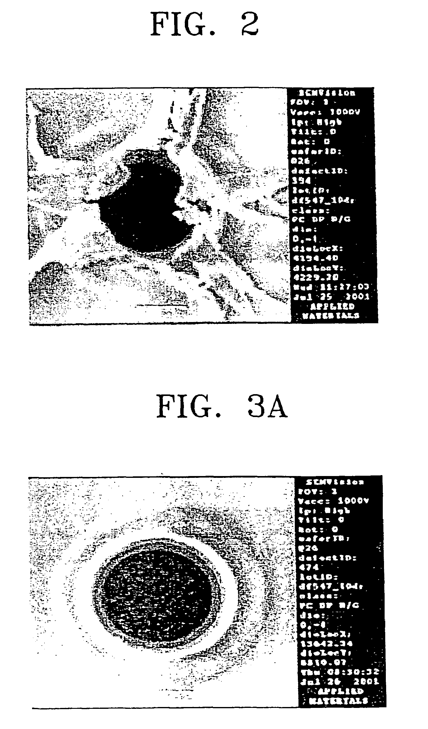
[0070]This example illustrates a performance comparison between the composition according to the present invention, the conventional stripper A, and another conventional organic stripper (to be referred to as a stripper B).

[0071]The via having a width of 400–500 μm was formed in the same manner as in Example 1, and then an ashing step was performed. The top view of the resultant via was observed using SEM and the observation results are shown in FIG. 2, where it is seen that a large amount of polymer remains around the via circumference.

[0072]The wafer subjected to the ashing step was dipped into the composition according to the present invention at 65° C. for 20 minutes, rinsed with deionized water and then dried. Thereafter, the top view and cross-sectional view of the via were observed using SEM and the observation results are shown in FIGS. 3A and 3B.

[0073]The wafers subjected to the ashing step were dipped into the strippers A and B at 65° C. for 20 minutes, rinsed with deioniz...


PUM

PropertyMeasurementUnit
Fractionaaaaaaaaaa
Fractionaaaaaaaaaa
Fractionaaaaaaaaaa

Abstract

A resist removing composition having a superior capability for removing a resist, polymer, organometallic polymer and etching by-products such as metal oxide, which does not attack underlying layers exposed to the composition and which does not leave residues after a rinsing step. The resist removing composition contains alkoxy N-hydroxyalkyl alkanamide and a swelling agent.

Description

[0001]This is a divisional of U.S. patent application Ser. No. 10 / 059,150, filed Jan. 31, 2002, now U.S. Pat. No. 6,713,440 the entire contents of each of which are hereby incorporated herein by reference for all purposes as if fully set forth herein.BACKGROUND OF THE INVENTION[0002]1. Field of the Invention[0003]The present invention relates to a resist or etching by-product removing composition and a resist removing method using the same.[0004]2. Description of the Related Art[0005]Semiconductor devices are manufactured via an elaborate series of discrete and sequential processes. After certain of these processes for manufacturing the semiconductor device, e.g., a dry etching process or an ion implantation process, a resist pattern that was used as a mask must be removed. Also, in the case when the resist pattern was misaligned, it must be removed to form a new and correctly aligned resist pattern.[0006]An important criterion of the resist removing process is to completely remove ...

Claims


Application Information

Patent Timeline
IPC IPC(8): B08B3/04G03F7/32C11D1/52C11D7/26C11D7/32C11D7/34C11D7/50C11D7/60C11D11/00G03F7/42H01L21/027H01L21/3065
CPCC11D1/526C11D11/0047G03F7/425C11D2111/22G03F7/32
Inventor PARK, DONG-JINKIM, KYUNG-DAECHON, SANG-MUNHWANG, JIN-HOSOHN, IL-HYUNPARK, SANG-OHJUN, PIL-KWON
Owner SAMSUNG ELECTRONICS CO LTD
Why Eureka
Try Eureka