Multi-channel laser pump source for optical amplifiers

a laser pump source and optical amplifier technology, applied in semiconductor lasers, optical elements, instruments, etc., can solve the problems of increasing affecting the overall cost of the amplifier, so as to reduce the number of manufacturing steps, facilitate the manufacturing process, and facilitate the manufacturing process. the effect of high efficiency coupling

Inactive Publication Date: 2007-06-26
GEMFIRE CORP
View PDF25 Cites 41 Cited by
  • Summary
  • Abstract
  • Description
  • Claims
  • Application Information

AI Technical Summary

Benefits of technology

[0019]Roughly described, a multiple output diode laser pump source is manufactured by an array scaleable optical alignment process, which can achieve simultaneous highly efficient coupling between each of the emitters in a laser diode array aid a respective receiving waveguide array. The waveguide array may be fabricated (without limitation) in a lithium niobate, glass substrate, or other integrated optics chip. The simultaneous coupling of all of the emitter / waveguide pairs advantageously reduces the number of manufacturing steps, thereby allowing the pump source to be manufactured more rapidly and inexpensively.
[0021]In addition, the standoff structure also can overcome other problems in the prior art by, for example, eliminating the effect of solder deposition thickness on emitter position, lessening the impact of foreign particulate defects by decreasing the contact area between the arrays and the submount, and alleviating the effects of non-uniform bonding pressure and chip bow or warp by distributing the reference surface across the entire array and therefore referencing the positions relative to the submount of all emitters directly to the same reference surface.

Problems solved by technology

However, this improved performance is typically accompanied by increased cost.
Thus the cost of the high performance EDFA is shared amongst many revenue generating data streams and subscribers.
A significant proportion of the overall cost of the amplifier results from the semiconductor diode laser pumps, which typically cost many thousands of dollars each.
The fully active fiber alignment process described above is both cumbersome and slow, and although it can result in remarkably good coupling efficiency between the diode laser and fiber (in excess of 60%), it does not lend itself well to high volume, high yield and low cost manufacturing.
It is this fully active alignment step that accounts for a significant portion of the cost of constructing a diode laser pump source for an EDFA.
Such prior art techniques do not provide the level of precision obtained using the active fiber alignment described above, and which is conventionally required to achieve efficient coupling between a diode laser and an optical fiber.
Difficulties include height variation (that is spacing between the diode laser chip and the substrate) across the lateral array dimension due to solder thickness variations or bonding pressure variations.
Thus, co-planarity of the bonding surfaces is difficult to achieve to the degree desired for very efficient coupling (typically about 0.2 microns over 10 mm for a high channel count laser diode array).
Bowing of the diode laser chip also gives rise to misalignments across an array of emitters.
Fabrication of the diode laser structure using epitaxial growth and planar surface lithography often results in a laser array chip with a residual bow or warpage.
In addition, misalignment can also be caused by particles trapped between the diode array and the mounting surface.
Keeping large planar surfaces free of particles is difficult.
This may help to minimize the effect of foreign particles, but does not address the absolute positioning of the multiple emitters across the array, and cannot alleviate misalignment arising from laser array curvature due to warped or bowed wafers.

Method used


Image

  • Multi-channel laser pump source for optical amplifiers
  • Multi-channel laser pump source for optical amplifiers
  • Multi-channel laser pump source for optical amplifiers

Examples


Embodiment Construction

[0051]The invention will now be described in reference to various non-limiting embodiments thereof. It should be noted that individual elements or features of different embodiments described below may be combined in various permutations to produce a laser pump source having a set of desired physical and / or operational characteristics, and that such combinations are within the scope of the present invention.

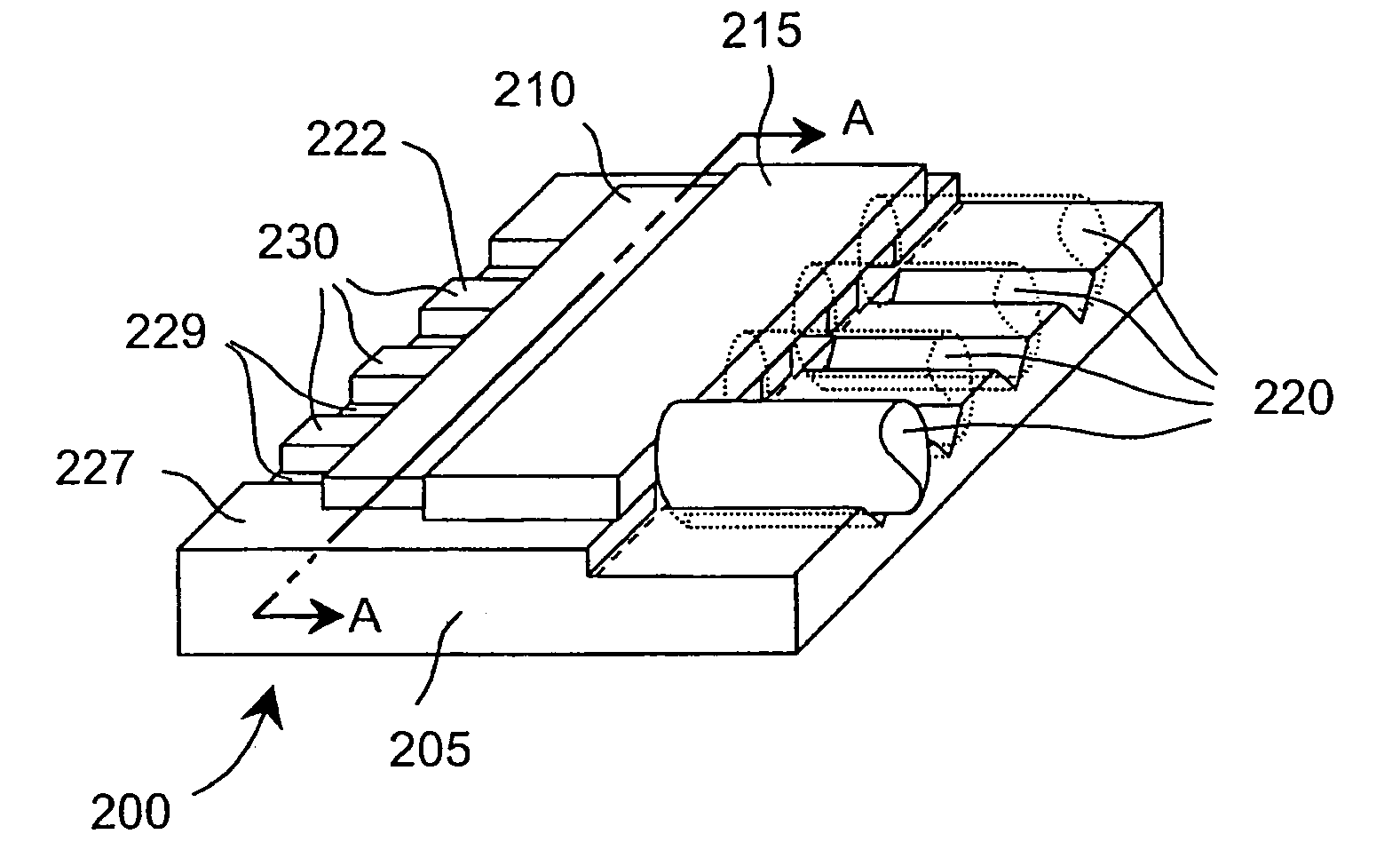
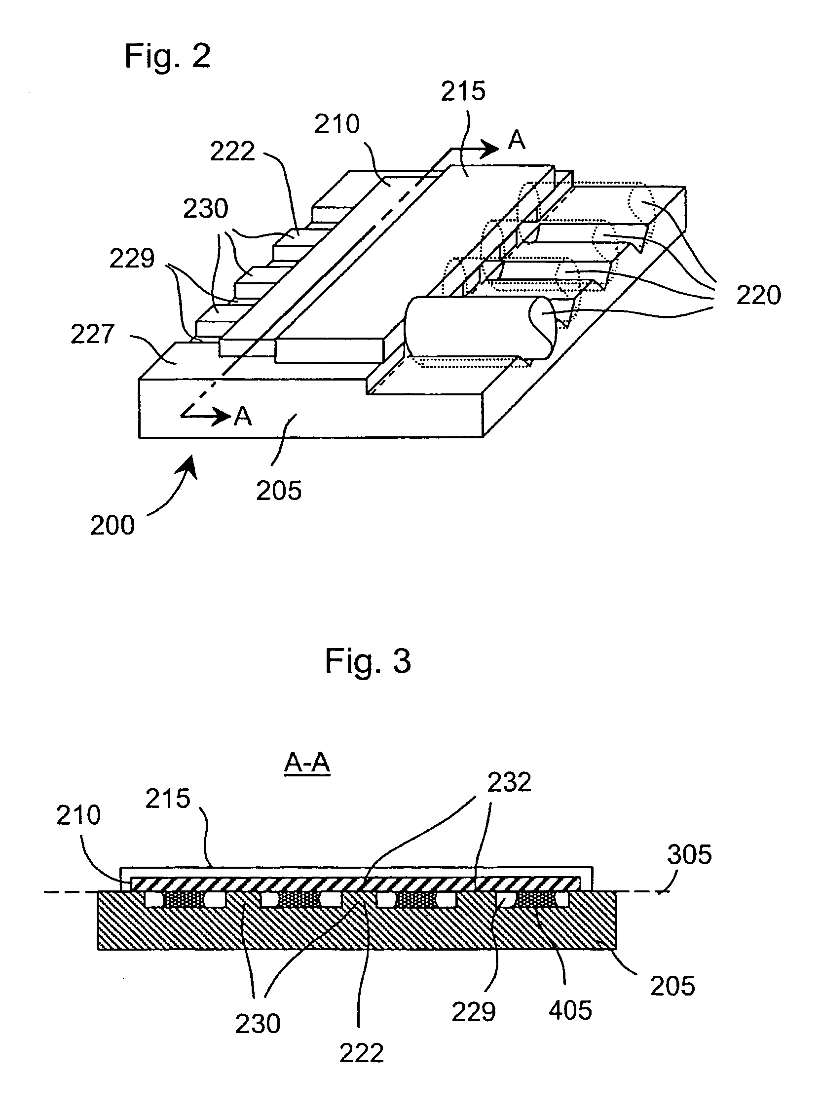
[0052]FIG. 2 illustrates an embodiment of a semiconductor diode laser pump source 200 in accordance with aspects of the invention. Pump source 200 is shown to include several major components: a submount 205, a diode laser array (hereinafter “laser array”) 210, an integrated optic (IO) waveguide chip 215 and an optical fiber array 220. As used herein, an optical “array” is a device that includes two or more optical ports. The submount 205, laser array 210 and IO chip 215 are shown in greater detail in FIG. 22, which illustrates in particular opposing edges 250 and 255 of laser arr...


PUM

PropertyMeasurementUnit
wavelengthsaaaaaaaaaa

Abstract

An optical assembly, such as a multiple output diode laser pump source for EDFAs, is formed by pressing an optical array emitter chip against a standoff structure protruding from a submount such that the emitter chip deforms to match the curvature of the standoff structure. An IO chip is also juxtaposed against the standoff structure such that its optical receivers can receive optical energy from the emitter chip. The IO chip can provide various optical functions, and then provide an optical array output for coupling into an optical fiber array. The standoff structure preferably contacts the emitter chip over an aggregate contact area much smaller than the area by which the emitter chip overlaps the submount. The materials used for bonding the emitter chip and the IO chip to the submount are disposed in the recesses between standoffs and not on the contact surfaces of the standoff structure.

Description

[0001]This application is a continuation of application Ser. No. 10 / 616,008, filed 9 Jul. 2003, now abandoned, which is a continuation of application Ser. No. 09 / 784,687, filed 14 Feb. 2001, now abandoned.BACKGROUND OF THE INVENTION[0002]1. Field of the Invention[0003]This invention relates generally to semiconductor diode laser based pump sources, and more specifically to techniques for construction of planar multi-channel diode laser pump sources.[0004]2. Description of Related Art[0005]Optical amplifiers are an accepted part of long-haul telecommunications systems. They are used to amplify signals after optical fiber propagation losses over long transmission distances typical of such as the nation-wide networks. A typical system uses a plurality of Erbium doped fiber amplifiers (EDFAs) pumped by semiconductor diode lasers. Semiconductor diode laser pump sources for EDFAs typically operate at wavelengths of 980 nanometers (nm) or 1480 nm. The EDFA is capable of amplifying waveleng...

Claims


Application Information

Patent Timeline
Patent Type & Authority Patents(United States)
IPC IPC(8): B32B37/10G02B6/30G02B6/42H01S3/0941H01S5/022H01S5/40
CPCG02B6/4201G02B6/4204G02B6/4232G02B6/4249H01S5/02252G02B6/30Y10T156/1089G02B6/362G02B6/3636G02B6/3652G02B6/3692G02B6/4202G02B6/4224G02B6/4225G02B6/423G02B2006/12195H01S3/09415H01S5/02284H01S5/141H01S5/146H01S5/4012H01S5/4062Y10T156/1093Y10T156/1028Y10T156/1092Y10T156/109G02B6/305H01L2224/48091G02B6/4286G02B6/4243G02B6/4265G02B6/4267G02B6/4287H01S5/02326H01S5/02251H01L2924/00014
Inventor BISCHEL, WILLIAM K.WAGNER, DAVID K.GUENTHER, HARALDFIELD, SIMON J.HEHLEN, MARKUS P.TOMPANE, RICHARD B.RYAN, ANDREW T.FANNING, C. GEOFFREYLI, JIM W.MOROZOVA, NINA D.
Owner GEMFIRE CORP
Why Eureka
Try Eureka