Process for assembling three-dimensional systems on a chip and structure thus obtained

a three-dimensional system and chip technology, applied in the field of process for fabricating electronic circuit devices, can solve the problems of costly development of customized processes for every component, limited number of different devices and material systems, and limited application range of both techniques, so as to achieve large gains in size, weight and performan

Inactive Publication Date: 2007-08-07
HRL LAB
View PDF53 Cites 96 Cited by
  • Summary
  • Abstract
  • Description
  • Claims
  • Application Information

AI Technical Summary

Benefits of technology

[0028]One of the most costly, time-consuming portions of satellite construction is the fabrication of the RF circuitry and support electronics. For each of the many communication channels carried on a satellite, a high-gain, low-noise receiver chain and a high-gain, high-power transmitter chain are needed. These chains contain dozens of discrete transistors, microwave-monolithic integrated circuits (MMIC), and passive microwave elements that are all painstakingly hand-assembled, which cover very large areas since they are based on 2-dimensional assembly techniques. The use of the heterogeneous integration method according to the present invention allows large gains in terms of size, weight, and performance of these RF assemblies.

Problems solved by technology

However, both of these techniques are limited in the number of different devices and material systems that can be successfully integrated.
Moreover, growth and fabrication procedures optimized for a single device technology often must be compromised to accommodate dissimilar material systems.
This forces the costly development of customized processes for every component and prevents the use of low-cost foundries for producing the integrated systems.
However, for the integration of a silicon substrate with group III-V semiconductor materials, components or devices, this process suffers from a large defect density caused by the mismatch in lattice parameters and by the fact that devices in the silicon substrate can only be fabricated through widely-separated “holes” in the epitaxial film.
In addition, only one type of III-V layer can be utilized, which means that applications that could benefit from both Gallium Arsenide (GaAs) and Indium Phosphide (InP) devices are not possible.
However, the large thermal expansion mismatch between III-V materials and silicon requires almost complete removal of the III-V substrate prior to interconnect formation or additional processing.
A further disadvantage is that wafer bonding techniques can only be used to add a single type of III-V device to silicon.
However, this approach also suffers from problems due to thermal expansion mismatch as well as thermal degradation of devices present in the silicon substrate during processing of the III-V layer.
However, flip-chip is limited to a two-dimensional planar geometry, resulting in large overall package size.
Moreover, this technique is inefficient for the placement of large numbers of components, since placement is performed serially.
However, these technologies are not usable for three-dimensional integration of active devices.
LTCC techniques require sintering at 850° C., which would destroy most processed semiconductor devices.
The HDMI technique utilizes multiple levels of flexible polymer films to achieve layer-to-layer interconnects, but does not provide a method for incorporating active devices within a layer.
Both LTCC and HDMI are inefficient for the placement of large numbers of components due to their serial nature.
A disadvantage of the gravity-based assembly methods is that they are limited to single-layer structures.
In fact, since this assembly method involves the filling of receptacle sites on a host substrate by shaped device blocks, it is limited to a two-dimensional assembly.
The reason for this limitation is that device blocks must have an unobstructed access to the receptacle sites.
Prior art approaches require device fabrication to take place after transfer or bonding on thin semiconductor layers, with the consequence of serious restrictions on the allowable device designs that can be employed.
One of the most costly, time-consuming portions of satellite construction is the fabrication of the RF circuitry and support electronics.

Method used


Image

  • Process for assembling three-dimensional systems on a chip and structure thus obtained
  • Process for assembling three-dimensional systems on a chip and structure thus obtained
  • Process for assembling three-dimensional systems on a chip and structure thus obtained

Examples


Embodiment Construction

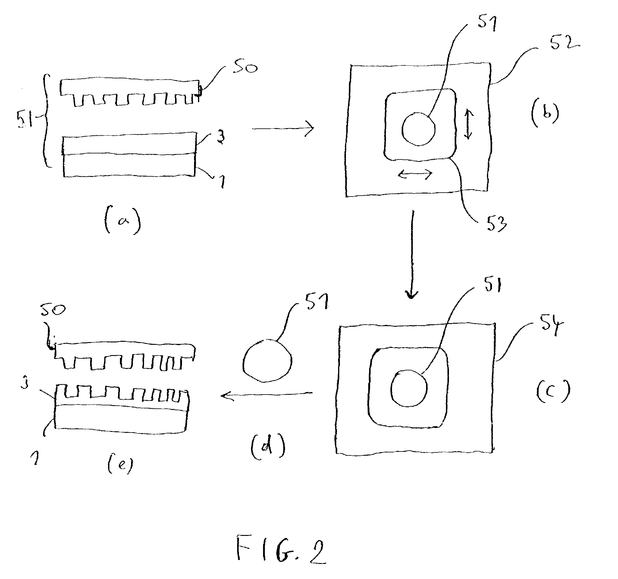
[0037]Reference now will be made to the drawings, which are used to aid in the description of preferred embodiments of the invention. However, the invention is not limited to the drawings or description presented herein.

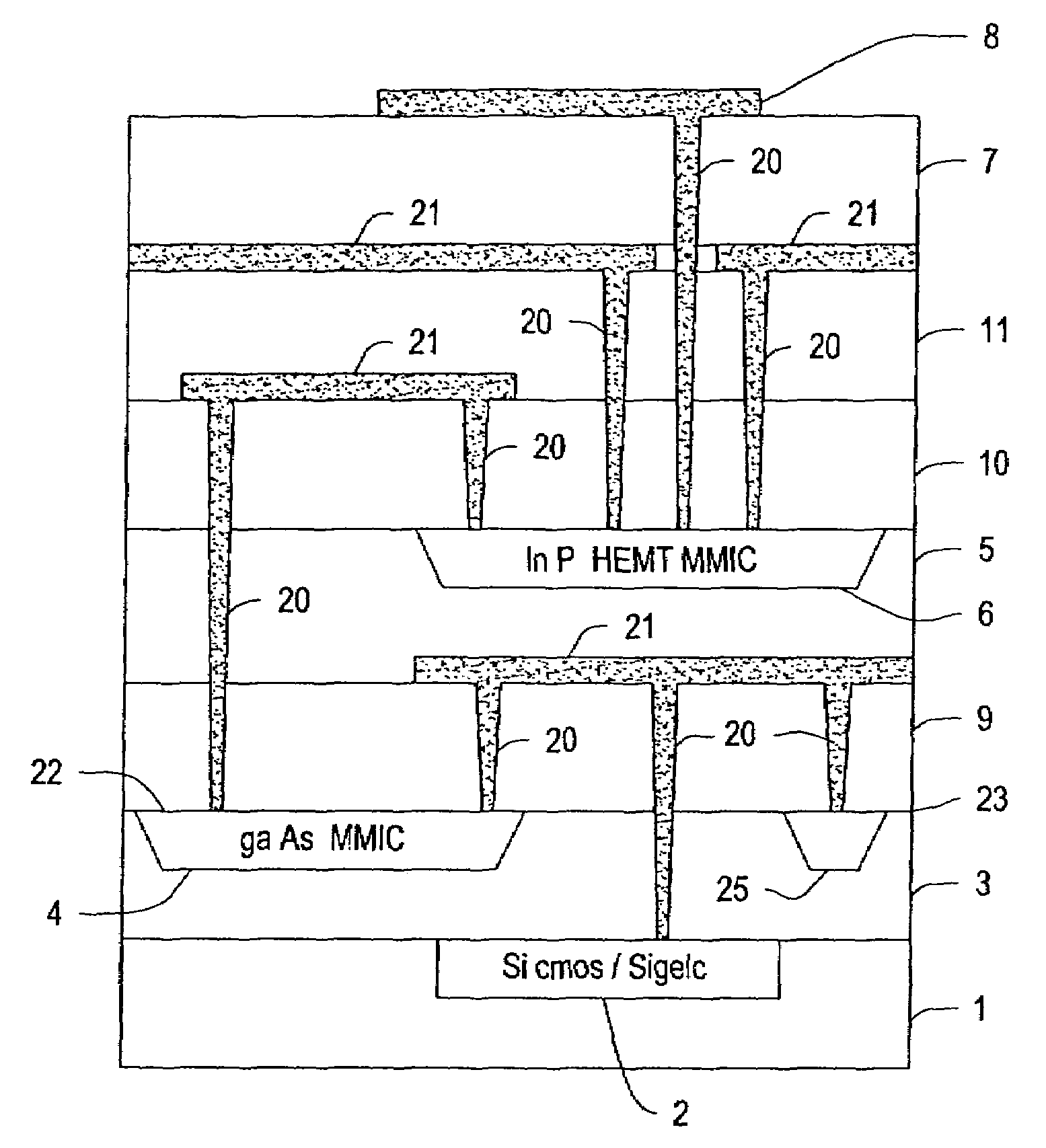
[0038]According to the present invention, multiple layers consisting of vertically-integrated electronic components, such as active RF device and sensor transducers (antennas, optical receivers, etc.) are stacked one over the other.

[0039]FIG. 1 shows a schematical cross-sectional view of an exemplary three-dimensional system architecture according to the present invention, referred to as an integrated transmit / receive module for RF applications.

[0040]A substrate 1, for example, a silicon substrate, contains a CMOS microcircuit 2, such as a high-performance Si / SiGe CMOS integrated circuit. The silicon substrate 1 forms the host circuit or base upon which multiple receptacle layers 3, 5 and 7 are registered. Each receptacle layer is capable of supporting components fab...


PUM


Abstract

A method for assembling an electronic system with a plurality of layers. Recesses in formed in one or more dielectric layers and electronic components are positioned within the recesses. One or more layers containing the components are placed on a host substrate containing host circuits. Electrical interconnects are provided between and among the electronic components in the dielectric layers and the host circuits. The layers containing the components may also be provided by growing the electronic devices on a growth substrate. The growth substrate is then removed after the layer is attached to the host substrate.

Description

CROSS-REFERENCE TO RELATED APPLICATIONS[0001]The present document is related to the cop ending and commonly assigned patent application documents entitled: “Process for Assembling Three-Dimensional Systems on a Chip and Structure Thus Obtained,” Ser. No. 60 / 326,076; “Process For Producing High Performance Interconnects,” Ser. No. 60 / 326,054; “Method For Assembly Of Complementary-Shaped Receptacle Site And Device Microstructures,” Ser. No. 60 / 326,055; and “Method of Self-Latching for Adhesion During Self-Assembly of Electronic or Optical Circuits,” Ser. No. 60 / 326,056, all of which were filed on Sep. 28, 2001. The contents of these related applications are hereby incorporated by reference herein.BACKGROUND[0002]1. Field[0003]The present disclosure relates to processes for fabricating electronic circuit devices, more particularly, the disclosure relates to a process for assembling three-dimensional systems on a chip and to the structure thus obtained.[0004]2. Description of Related Ar...

Claims


Application Information

Patent Timeline
Patent Type & Authority Patents(United States)
IPC IPC(8): H01L21/4763H01L23/34G06F17/50H01L21/44H01L21/48H01L21/50H01L21/822H01L21/8258H01L23/52H01L27/06H01L27/10H01L29/40
CPCH01L21/6835H01L21/8221H01L21/8258H01L24/24H01L24/82H01L24/95H01L25/50H01L27/0605H01L27/0688H01L2924/1305H01L2924/13064Y10S438/928H01L2221/68345H01L2221/6835H01L2224/24145H01L2224/95085H01L2924/01013H01L2924/01027H01L2924/01039H01L2924/01049H01L2924/01078H01L2924/01079H01L2924/04953H01L2924/09701H01L2924/10253H01L2924/10329H01L2924/14H01L2924/1423H01L2924/3011H01L2924/01005H01L2924/01006H01L2924/01019H01L2924/01023H01L2924/01024H01L2924/01033H01L2924/014H01L2924/00H01L2924/15153H01L2924/15155
Inventor BREWER, PETER D.CASE, MICHAEL G.HUNTER, ANDREW T.MATLOUBIAN, MEHRANROTH, JOHN A.POBANZ, CARL W.
Owner HRL LAB
Why Eureka
Try Eureka