
Silicon-on-sapphire display with audio transducer and method of fabricating same

a technology of liquid crystal displays and audio transducers, which is applied in non-linear optics, instruments, optics, etc., can solve the problems of limiting the integration of display driving circuitry heretofore to thin film transistors, and fabricating the displays on transparent glass or quartz substrates

Inactive Publication Date: 2007-08-07
NAVY UNITED STATES OF AMERICA AS REPRESENTATED BY THE SEC OF THE THE
View PDF6 Cites 37 Cited by
  • Summary
  • Abstract
  • Description
  • Claims
  • Application Information

AI Technical Summary

Benefits of technology

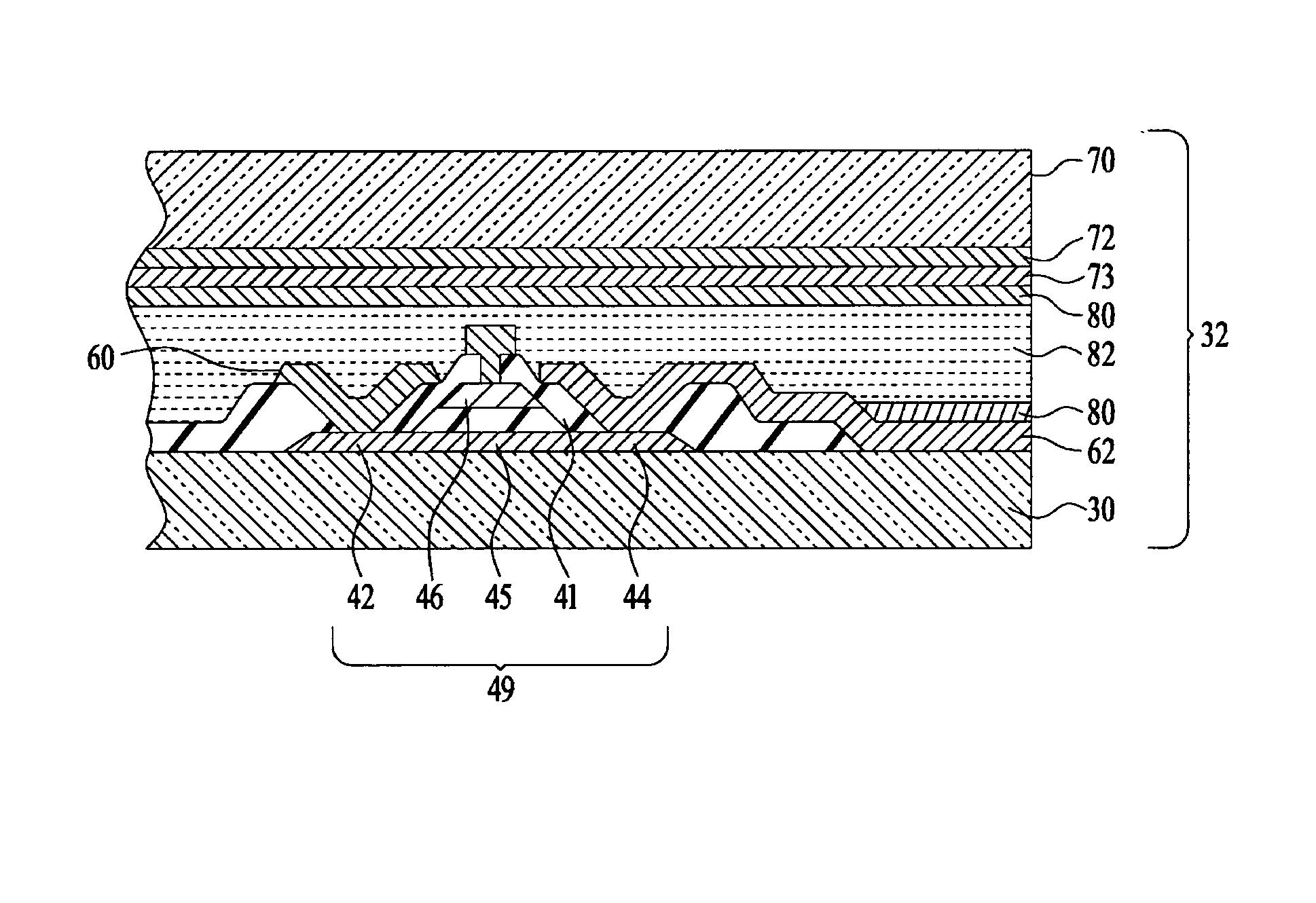
"The invention is a liquid crystal display system that includes a sapphire substrate and a silicon structure with liquid crystal capacitors and integrated circuitry for generating a video and audible signal. The system also includes an audio transducer for generating the audible signal. The method of fabrication involves ion implantation, annealing, oxidation, and patterning of silicon layers to create the transistors and electrical contacts. The invention allows for the fabrication of a monolithically integrated crystal array display and control circuitry on a silicon-on-sapphire structure. The technical effects include improved image quality and reduced power consumption."

Problems solved by technology

Limitations inherent in the existing technology come from the necessity of fabricating the displays on transparent glass or quartz substrates, which are not amenable to high quality electronic materials.
Fabrication of displays on bulk silicon, although of high crystal quality, unnecessarily constrains the display to reflective mode schemes due to the opaque substrate and is not applicable to transmissive applications.
However, the integration of display driving circuitry heretofore has been substantially limited to thin film transistor technology using amorphous (a-Si) or polycrystalline (p-Si) silicon deposited on the glass or quartz substrate.
The intrinsic properties such as lattice and thermal mismatch between the silicon layer and the substrate, and the low temperature deposition techniques used in the a-Si and p-Si technologies result in a silicon layer with poor charge carrier mobility and crystallographic defects.
These limitations are directly related to inferior electronic device performance and limitations when compared to bulk silicon.
The characteristic lower (electrical and crystallographic) qualities of a-Si and p-Si materials result in poor fabrication yields when compared to conventional Very Large Scale Integration (VLSI) processing.
This redundancy requires a concomitant increase in the picture element (pixel) size thereby inhibiting the ability to scale displays and light valves to ultra-high resolution.
The additional circuit elements also reduce the aperture ratio, i.e. the fraction of pixel area allowing transmitted light, thereby reducing the brightness of the display or light valve.
Furthermore, the low carrier mobility, low speed, low yield a-Si and p-Si materials are incompatible with VLSI design and fabrication techniques which would otherwise readily allow integration of video drivers, digital logic and other computational circuitry on-chip thereby offering designers greater functionality, higher reliability, and improved performance.

Method used


Image

  • Silicon-on-sapphire display with audio transducer and method of fabricating same
  • Silicon-on-sapphire display with audio transducer and method of fabricating same
  • Silicon-on-sapphire display with audio transducer and method of fabricating same

Examples


Embodiment Construction

[0017]Following is a glossary of terms used to describe the Silicon-On-Sapphire Display With Audio Transducer and Method of Fabricating Same. The definitions set forth in the glossary are representative of the intended meanings as used herein.

Glossary

[0018]The term “audible” means capable of being heard; typically by an average human ear; including frequencies normally in the range of about 15 to about 20,000 hertz.

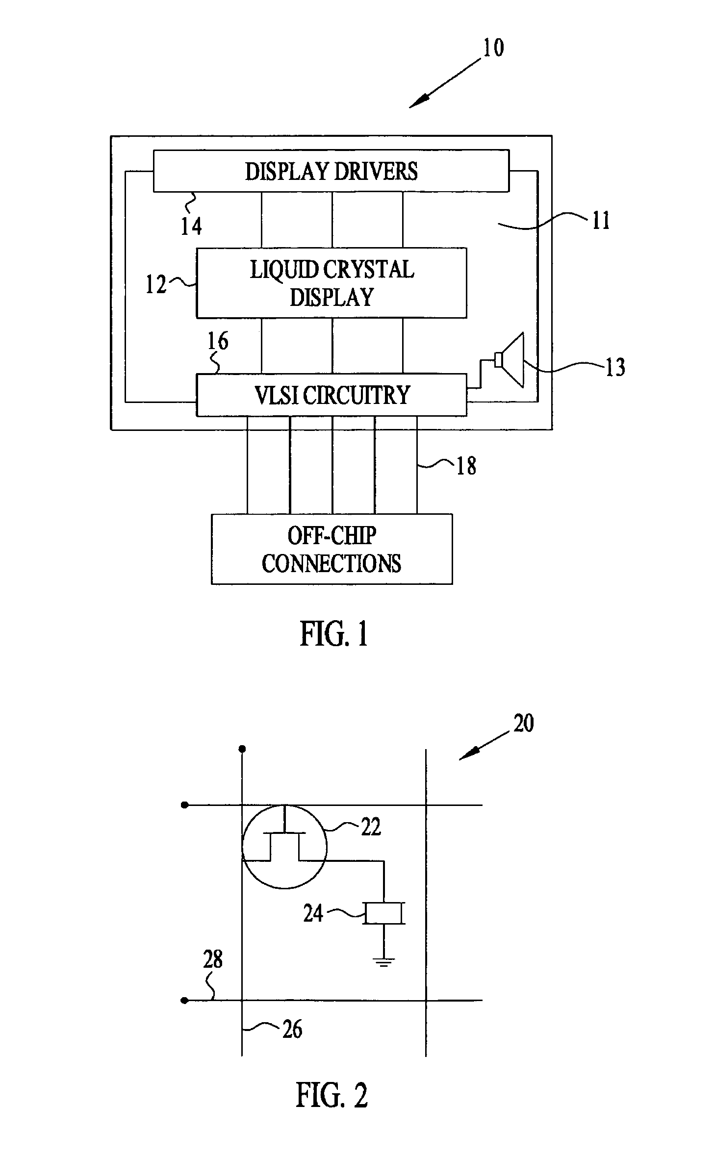
[0019]FIG. 1 shows a SOS display 10. Display 10 includes nematic liquid crystal display 12, display drivers 14, very large scale integration (VLSI) circuitry 16, and audio transducer 13 monolithically integrated on an improved ultra-thin silicon-on-sapphire (UTSOS) wafer 11.

[0020]Liquid crystal display 12 includes an array of one or more pixel elements, which may be individually addressed so that display 12 presents an image for viewing or projection. By way of example, a 1000 pixel×1000 pixel display may be incorporated into display 12, but it is recognized that any numb...


PUM

PropertyMeasurementUnit
thicknessaaaaaaaaaa
frequenciesaaaaaaaaaa
temperatureaaaaaaaaaa

Abstract

A liquid crystal display includes: a) a sapphire substrate; b) a single crystal silicon structure disposed on the sapphire substrate to create a silicon-on-sapphire structure; c) a plurality of liquid crystal capacitors disposed on the silicon-on-sapphire structure; d) integrated self-aligned circuitry formed from the crystal silicon structure, where the circuitry modulates the liquid crystal capacitors such that a video image is generated; and e) an integrated audio transducer disposed on the silicon-on-sapphire structure for generating an audible signal.

Description

CROSS-REFERENCE TO RELATED APPLICATIONS[0001]This application is a continuation-in-part of U.S. patent application Ser. No. 10 / 614,426 (Navy Case No. 84,892) filed Jul. 7, 2003 now U.S. Pat. No. 6,954,235, entitled “Silicon-On-Sapphire Display Apparatus And Method of Fabricating Same,” which is a continuation-in-part of U.S. patent application Ser. No. 09 / 880,660 (Navy Case No. 83,222) filed Aug. 3, 2001 now U.S. Pat. No. 6,6617,187, entitled “Method For Fabricating An Electrically Addressable Silicon-On-Sapphire Light Valve,” which is a divisional of U.S. patent application Ser. No. 09 / 047,658 (Navy Case No. 79,029) filed Mar. 25, 1998 now U.S. Pat. No. 6,312,968, entitled “Method For Fabricating An Electrically Addressable Silicon-On-Sapphire Light Valve,” which is a continuation-in-part of U.S. patent application Ser. No. 08 / 301,170 (Navy Case No. 74,146) filed Sep. 1, 1994 (abandoned), entitled “Method For Fabricating An Electrically Addressable Silicon-On-Sapphire Light Valve,”...

Claims


Application Information

Patent Timeline
Patent Type & Authority Patents(United States)
IPC IPC(8): G02F1/1333G02F1/1343G02F1/1362
CPCG02F1/13454
Inventor RUSSELL, STEPHEN D.SHIMABUKURO, RANDY L.OFFORD, BRUCE W.
Owner NAVY UNITED STATES OF AMERICA AS REPRESENTATED BY THE SEC OF THE THE
Learn More