Heat treatment apparatus and heat treatment method of substrate

a heat treatment apparatus and substrate technology, applied in glass tempering apparatus, manufacturing tools, instruments, etc., can solve the problems of high defect rate, difficult semiconductor device manufacturing, and inability to obtain thin-film transistors, so as to prevent deterioration in parts, easy to form semiconductor elements, and good substrate characteristics

Active Publication Date: 2007-08-14
DAINIPPON SCREEN MTG CO LTD
View PDF32 Cites 27 Cited by
  • Summary
  • Abstract
  • Description
  • Claims
  • Application Information

AI Technical Summary

Benefits of technology

[0017]Thus, it becomes possible to carry out a heat treatment process uniformly on the silicon film by using light irradiation, and consequently to relatively easily form a semiconductor element such as a thin-film transistor having constant and good characteristics on the substrate.
[0020]Thus, it is possible to carry out a heat treatment process uniformly by using light irradiation onto the silicon film, and consequently to relatively easily form a semiconductor element such as a thin-film transistor having constant and good characteristics on a substrate.
[0022]Since neither the pre-heating part nor the flash heating part is exposed to irradiation light mutually emitted from each other, it is possible to prevent deterioration in the parts.
[0023]Therefore, an object of the present invention is to provide a heat treatment method and apparatus for a substrate, which can relatively easily form a semiconductor element such as a thin-film transistor having constant and good characteristics on the substrate.
[0024]Another object of the present invention is to provide a heat treatment apparatus which can carry out stable operations while suppressing deterioration in the parts.

Problems solved by technology

However, the following problems have been raised in the conventional example having such an arrangement.
For this reason, it is not possible to obtain a thin-film transistor, etc. having desired transistor characteristics stably unless the laser irradiation energy is controlled with extremely high precision upon practical use at the time of the laser annealing process.
In other words, the application of standard laser irradiation apparatuses, etc. currently used widely makes it difficult to manufacture a semiconductor device including a thin-film transistor, etc. having desired transistor characteristics, and tends to cause malfunctions in the resulting semiconductor device and a higher rate of defective products.
Moreover, in the case of a lamp annealing process using a halogen lamp, the light-emitting energy of a light-emitting area to be absorbed in a silicon film is not sufficiently high, and it is necessary to provide a means for increasing light intensity or for making the irradiation time longer in order to carry out a sufficient process.
However, such a method increases not only the temperature of the silicon film on the glass substrate but also the temperature of the glass substrate to a level exceeding the necessary temperature, resulting in a warp and a distortion in the substrate.
However, in the case when the flash light is applied so as to raise the temperature of the surface of the substrate, the flash light and heat radiation that have passed through the substrate tend to cause burning of a filament and degradation in the lamp of the pre-heating part.

Method used


Image

  • Heat treatment apparatus and heat treatment method of substrate
  • Heat treatment apparatus and heat treatment method of substrate
  • Heat treatment apparatus and heat treatment method of substrate

Examples


first embodiment

1. First Embodiment

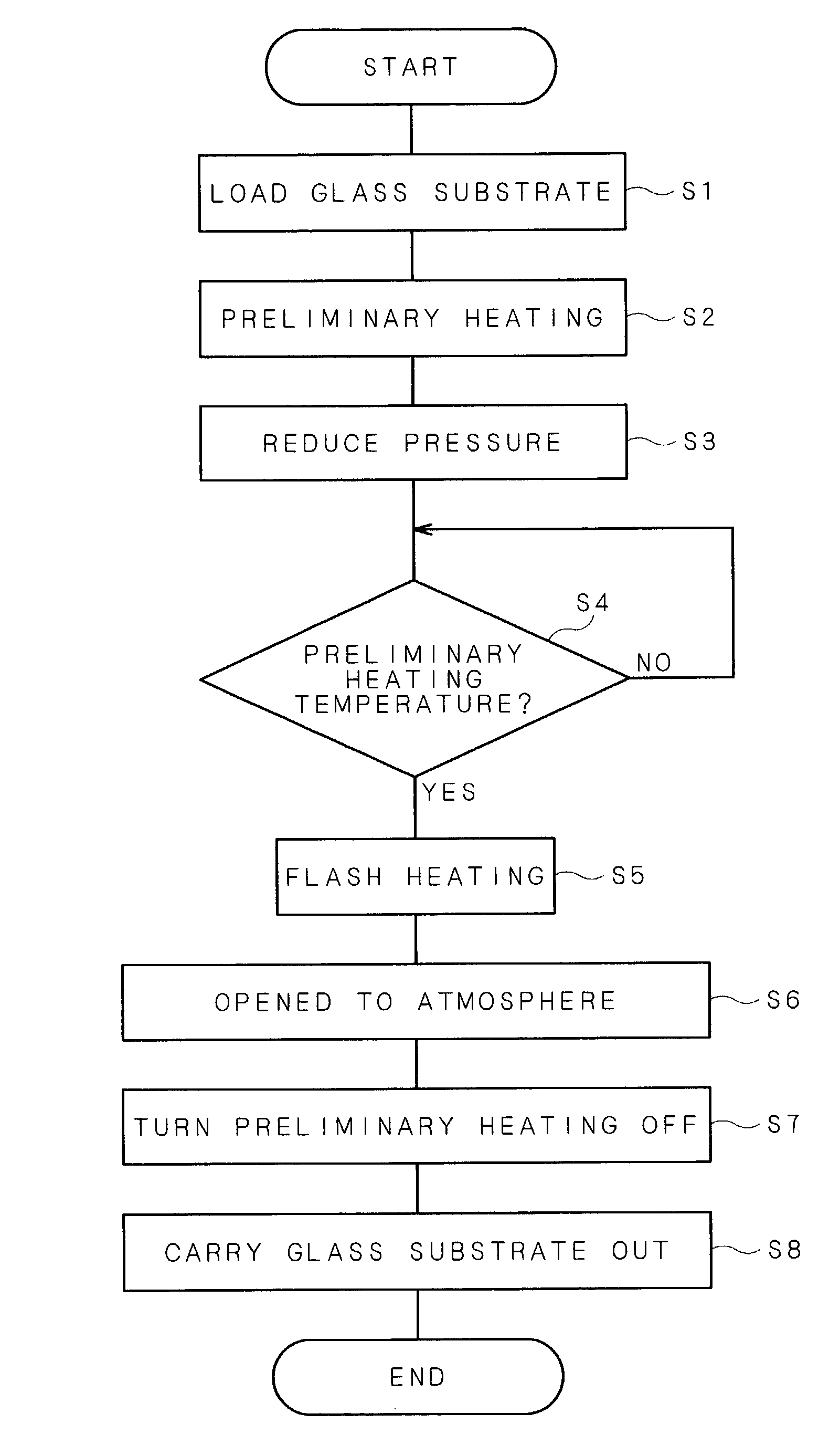
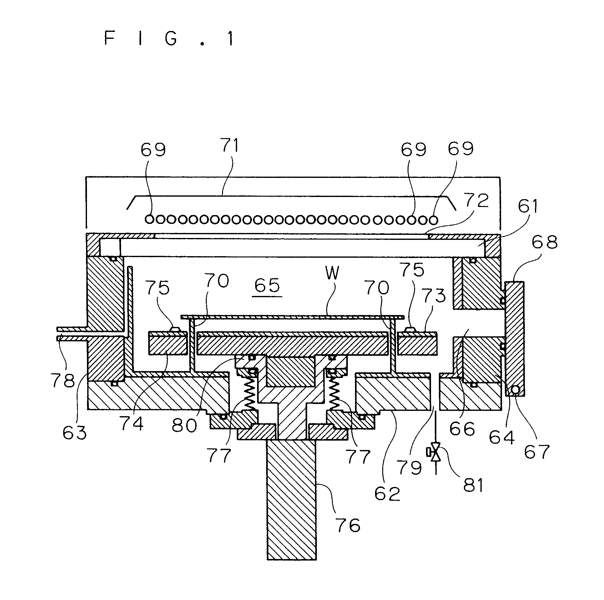
[0040]FIGS. 1 and 2 are cross-sectional views of a heat treatment apparatus in accordance with a first embodiment of the present invention, and FIG. 3 is a schematic plan view thereof.

[0041]This heat treatment apparatus is constituted by a translucent plate 61, a bottom plate 62 and a pair of side plates 63, 64, and provided with a heat treatment chamber 65 in which a glass substrate W bearing an amorphous silicon film formed thereon is housed and subjected to a heat treatment thereon. The translucent plate 61 constituting the heat treatment chamber 65 is made of a material such as quartz having an infrared-ray transmitting property. Moreover, supporting pins 70, which penetrates a heat diffusion plate 73 and a heating plate 74, which will be described later, and supports the glass substrate W from its lower face, are formed on the bottom plate 62 constituting the heat treatment chamber 65 in a manner so as to stick out therefrom.

[0042]Moreover, an opening section...

second embodiment

2. Second Embodiment

[0079]FIG. 7 shows a cross-sectional view of a heat treatment apparatus in accordance with a second embodiment of the present invention, and FIG. 8 is a schematic plan view thereof. Further, FIG. 9 is an enlarged view showing the inside of the heat treatment apparatus of the second embodiment.

[0080]This heat treatment apparatus, which is constituted by an upper plate 161, a bottom plate 162 and a pair of side plates 163, 164, is provided with a heat treatment chamber 165 which houses a glass substrate W having an amorphous silicon film formed thereon as a substrate to be treated therein, and caries out a heating treatment thereon. The respective plates 161, 162, 163, 164 constituting the heat treatment chamber 165 are made of a material, for example, stainless steel, and the surface of each of the plates is polished so as to prevent deformation due to heat radiation during the heat treatment process by flash light, which will be described later. Moreover, a trans...

third embodiment

3. Third Embodiment

[0130]Referring to FIG. 13, the following description will discuss a third embodiment of the present invention. FIG. 13 is an enlarged view that shows an essential portion of the inside of a heat treatment apparatus in accordance with the third embodiment.

[0131]In this arrangement, a flash heating part 180 and a pre-heating part 190 are not placed in a tilted manner in the same direction (upstream side in the transporting direction F in the second embodiment) with respect to a normal line L2 in light irradiation area M1, and the pre-heating part 190 is placed at a position dislocated from hypothetical line L1 of the flash heating part 180 so that these are not exposed to the mutual irradiation light rays. With this arrangement, the first detector 195 can be placed in the proximity of the flash heating part 180 on the surface side of the glass substrate W; therefore, the layout position forms a position that is hardly susceptible to influences of the irradiation li...


PUM

PropertyMeasurementUnit
thicknessaaaaaaaaaa
temperatureaaaaaaaaaa

Abstract

A heat diffusion plate and a heating plate are placed in a heat treatment chamber in this order. The heating plate is used for preliminarily heating a glass substrate to a temperature in a range from 200° C. to 400° C. The glass substrate thus preliminarily heated is subjected to a heat treatment by flash light irradiation by a xenon flash lamp. The flash light irradiation makes it possible to uniformly heat an amorphous silicon film on the glass substrate, and consequently to be poly-crystallized. Thus, it becomes possible to provide a heat treatment technique capable of carrying out a uniform heat treatment on the silicon film on the glass substrate sufficiently.

Description

BACKGROUND OF THE INVENTION[0001]1. Field of the Invention[0002]The present invention relates to a heat treatment method and an apparatus for a substrate, which improve characteristics of the substance by applying light thereto and are preferably used, in particular, when an amorphous silicon film is formed into a polycrystalline film upon manufacturing a semiconductor substrate and a thin-film transistor (TFT) or the like to be used for a liquid crystal display apparatus.[0003]2. Description of the Background Art[0004]A small-size, high precision active-matrix-type liquid crystal display (LCD) panel, which uses a polycrystalline silicon thin-film transistor (TFT) as its switching element, has been developed for use in a high-resolution display. The application of a polysilicon TFT to an active element of an LCD makes it possible to form a pixel array unit and a driving array unit on the same transparent insulating substrate in the same process; thus, the resulting advantage is that...

Claims


Application Information

Patent Timeline
Patent Type & Authority Patents(United States)
IPC IPC(8): B05D3/06B05D3/02H01L21/00
CPCH01L21/67115
Inventor KUSUDA, TATSUFUMI
Owner DAINIPPON SCREEN MTG CO LTD
Why Eureka
Try Eureka