Integrated monolithic tri-axial micromachined accelerometer

a micromachined accelerometer and integrated technology, applied in the field of sensors, can solve the problems of limiting the design flexibility of electrostatic actuators and capacitive sensors, affecting the performance of capacitive sensor designs, and affecting the safety of integrated circuits

Inactive Publication Date: 2007-08-21
UNIV OF FLORIDA RES FOUNDATION INC
View PDF20 Cites 131 Cited by
  • Summary
  • Abstract
  • Description
  • Claims
  • Application Information

AI Technical Summary

Benefits of technology

[0075]It is to be understood that while the invention has been described in conjunction with the preferred specific embodiments thereof, that the foregoing description as well as the examples which follow are intended to illustrate and not limit the scope of the invention. Other aspects, advantages and modifications within the scope of the invention will be apparent to those skilled in the art to which the invention pertains.

Problems solved by technology

Even though HF vapor can be used for release, protection of integrated circuits and sticking problems during release still remain major concerns.
Wiring on a single polysilicon microstructure is constrained to one electrode for each continuous microstructure which limits the design flexibility for electrostatic actuators and capacitive sensors.
Moreover, the relatively large parasitic capacitance in polysilicon processes degrades performance of capacitive sensor designs.
However, typically no CMOS circuitry is integrated on the sensor chip.
By assembling and orienting orthogonally two or three separate accelerometers, tri-axial acceleration sensing systems can be obtained, but both the package size and cost is high.
Among them, bulk micromachined 3-axis accelerometers generally have large mass, but require wafer bonding, wet etching and two-side alignment.
Significantly, the inherent large parasitic capacitance greatly reduces the obtainable signal-to-noise ratio.
The residual stress of the thin-film materials also limits the size of the proof mass which limits the obtainable resolution of the Lemkin's accelerometer.

Method used


Image

  • Integrated monolithic tri-axial micromachined accelerometer
  • Integrated monolithic tri-axial micromachined accelerometer
  • Integrated monolithic tri-axial micromachined accelerometer

Examples


example 1

Example 1

Structural Simulation

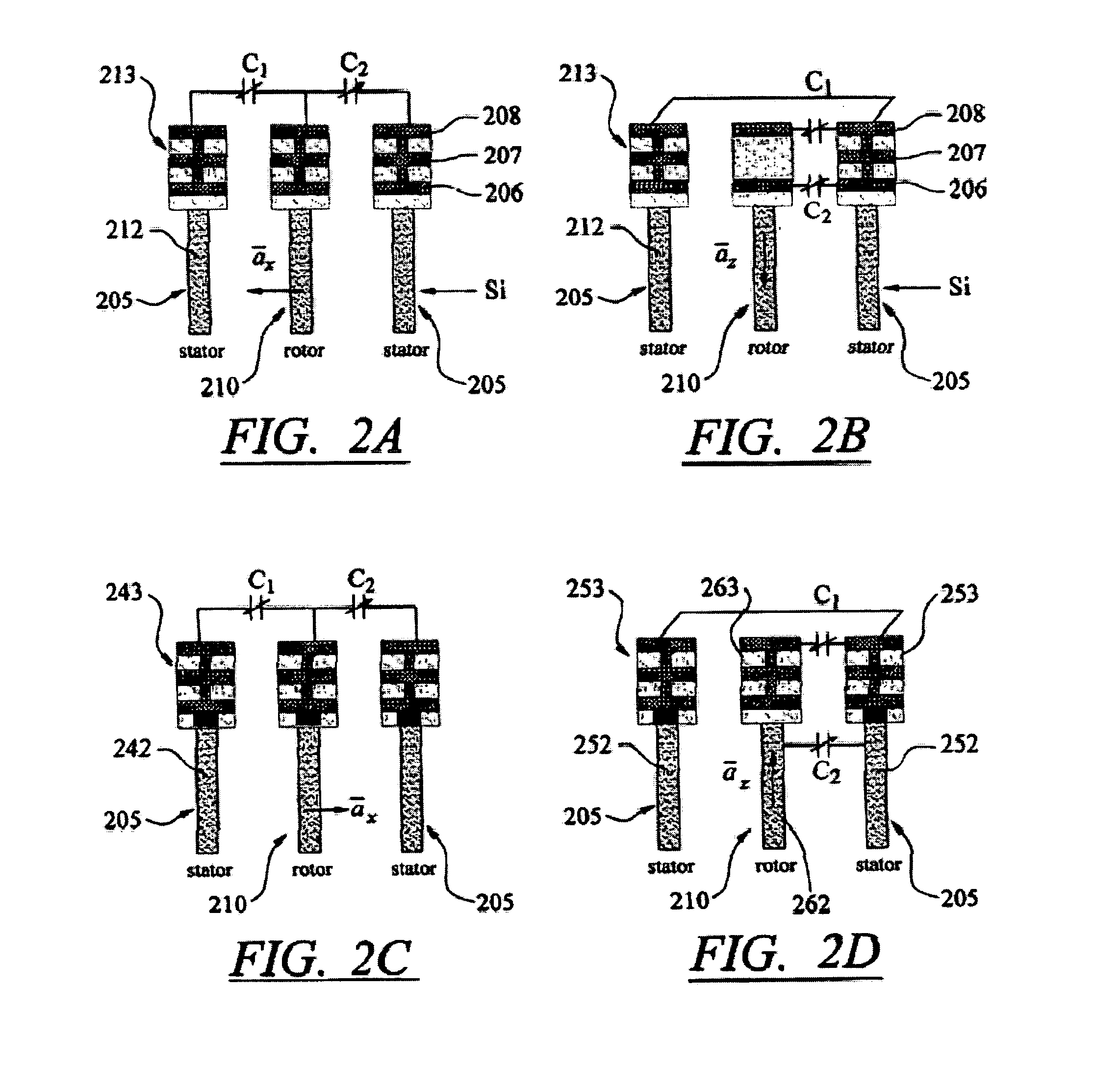
[0069]A structural simulation of a monolithic integrated three axis accelerometer according to an embodiment of the invention was performed using Nodal Design of Actuators and Sensors (NODAS) software. NODAS is a hierarchical cell library for behavioral modeling and nodal simulation of MEMS, was used [Q. Jing and G. K. Fedder, “A hierarchical circuit-level design methodology for microelectromechanical systems,” IEEE Transactions on Circuits and Systems II, Vol. 46 (1999), pp. 1309-1315]. NODAS consists of symbols and models of elements commonly found in suspended MEMS designs, such as anchors, beams, plates and gaps. As shown in FIGS. 2(A) and 2(B), the cross-section of the DRIE beams is not rectangular. A DRIE beam has a wider CMOS layer on top of the silicon layer. This irregular cross section has been considered and adopted in the DRIE beam model in the NODAS library.

[0070]FIG. 6(A) shows the NODAS model for an x-y accelerometer which includes x / y sp...

example 2

Example 2

Fabrication Results

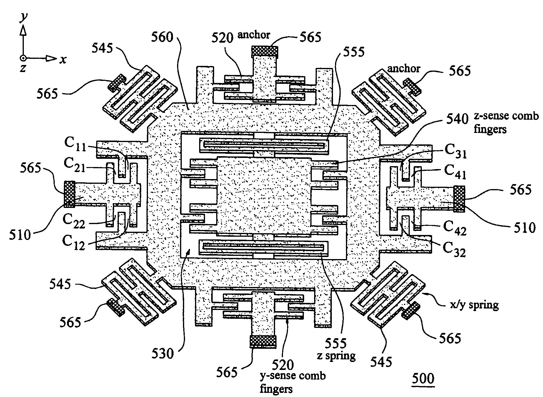
[0073]A released exemplary monolithic integrated three axis accelerometer 700 according to an embodiment of the invention is shown in FIG. 7(A) comprising x-sensing accelerometer 710, y-axis accelerometer 720 and z-axis accelerometer 730, all disposed on the same chip. The x-axis accelerometer 710 y-axis accelerometer 720 are identical and orthogonally oriented, while the z-accelerometer 730 is embedded in the center of accelerometer 700. The entire microstructure shown is about 1 mm by 1 mm in size. The SCS membrane layer was about 60 μm thick. Silicon underneath the z-spring beams 740 was completely undercut to maximize the z-compliance. Silicon underneath the x / y-spring beams 750 was just partially undercut to maintain the flatness of the whole structure. The silicon undercut on the comb fingers with small gaps was significantly reduced because of the known microloading effect.

[0074]FIG. 7(B) shows a micrograph of an x / y spring 750, while FIG. 7(C) sho...


PUM


Abstract

A monolithic integrated 3-axis accelerometer chip includes a single crystal substrate, the substrate including at least one single crystal membrane layer portion. A single sensor microstructure made from the single crystal membrane senses acceleration in each of the three orthogonal directions. At least one electronic circuit can also be disposed on the chip, such as a circuit for driving, detecting, controlling and signal processing.

Description

CROSS-REFERENCE TO RELATED APPLICATIONS[0001]This application is a continuation of U.S. patent application Ser. No. 10 / 786,787 now abandoned entitled “INTEGRATED MONOLITHIC TRI-AXIAL MICROMACHINED ACCELEROMETER” filed on Feb. 24, 2004, which claims the benefit of U.S. Provisional Application No. 60 / 449,745 entitled “INTEGRATED MONOLITHIC TRI-AXIAL MICROMACHINED ACCELEROMETER” filed on Feb. 24, 2003, the entirety of which is incorporated herein by reference.STATEMENT REGARDING FEDERALLY SPONSORED RESEARCH OR DEVELOPMENT[0002]The United States Government has rights in this invention pursuant to Agreements No. F30602-99-2-0545 and F30602-97-2-0323 between DARPA and Carnegie Mellon University.FIELD OF THE INVENTION[0003]The invention relates to sensors, and more particularly to monolithic integrated MEMS sensors.BACKGROUND[0004]Micromachined devices fabricated by complementary metal-oxide-semiconductor (CMOS)-compatible fabrication processes are attractive because of the ability to inte...

Claims


Application Information

Patent Timeline
Patent Type & Authority Patents(United States)
IPC IPC(8): G01P15/125A63B71/06B81B3/00G01P15/08G01P15/18
CPCB81B3/0062B81C1/00246G01P15/0802G01P15/125G01P15/18H03H9/02338B81B2201/0235B81C2203/0728G01P2015/082
Inventor XIE, HUIKAI
Owner UNIV OF FLORIDA RES FOUNDATION INC
Why Eureka
Try Eureka