Systems and methods for measuring stress in a specimen

a specimen and stress technology, applied in the direction of optical radiation measurement, semiconductor/solid-state device testing/measurement, instruments, etc., can solve the problems of thin film and/or substrate damage, substrate warpage, and no longer viable for manufacturing semiconductor devices

Inactive Publication Date: 2007-09-25
KLA TENCOR TECH CORP
View PDF31 Cites 23 Cited by
  • Summary
  • Abstract
  • Description
  • Claims
  • Application Information

AI Technical Summary

Benefits of technology

[0023]In another embodiment, the method may also include determining one or more geometrical parameters of the patterned structures using output generated by the optical technique. In one such embodiment, determining the stress may include determining the one or more geometrical parameters and the stress substantially simultaneously using a model describing effects of variations in the one or more geometrical parameters and the stress on polarization change in light used by the optical technique.
[0024]In another embodiment, the method may include monitoring one or more processes used to fabricate the patterned structures. In a further embodiment, the method may include controlling one or more processes used to fabricate the patterned structures using, for example, a fee...

Problems solved by technology

If the stress in either the thin film or the substrate becomes too high, then the thin film and/or the substrate may be damaged.
For instance, the thin film may crack and pull away from the wafer thereby necessitating removal and re-formation of the thin film on the substrate.
In another example, the substrate may become so warped that it is no longer viable for use in manufacturing semiconductor devices.
For example, wafers that are warped may be unsuitable for lithography processes since the focus of the exposure tool will vary across the wafer due to the differences in the position of the uppermost surface of the wafer caused by the warping.
Although the systems described by Wei et al. may be useful for measuring stress and other parameters of thin films, these systems do have some limitations.
For instance, these systems are not suitable for measuring stress in patterned structures formed on a wafer.
In particular, the bow and warp measurements may not represent the stress on patterned structures since the bow and warp measurements are performed across a relatively large area of the wafer and therefore may not accurately reflect the stress p...

Method used


Image

  • Systems and methods for measuring stress in a specimen
  • Systems and methods for measuring stress in a specimen
  • Systems and methods for measuring stress in a specimen

Examples


Embodiment Construction

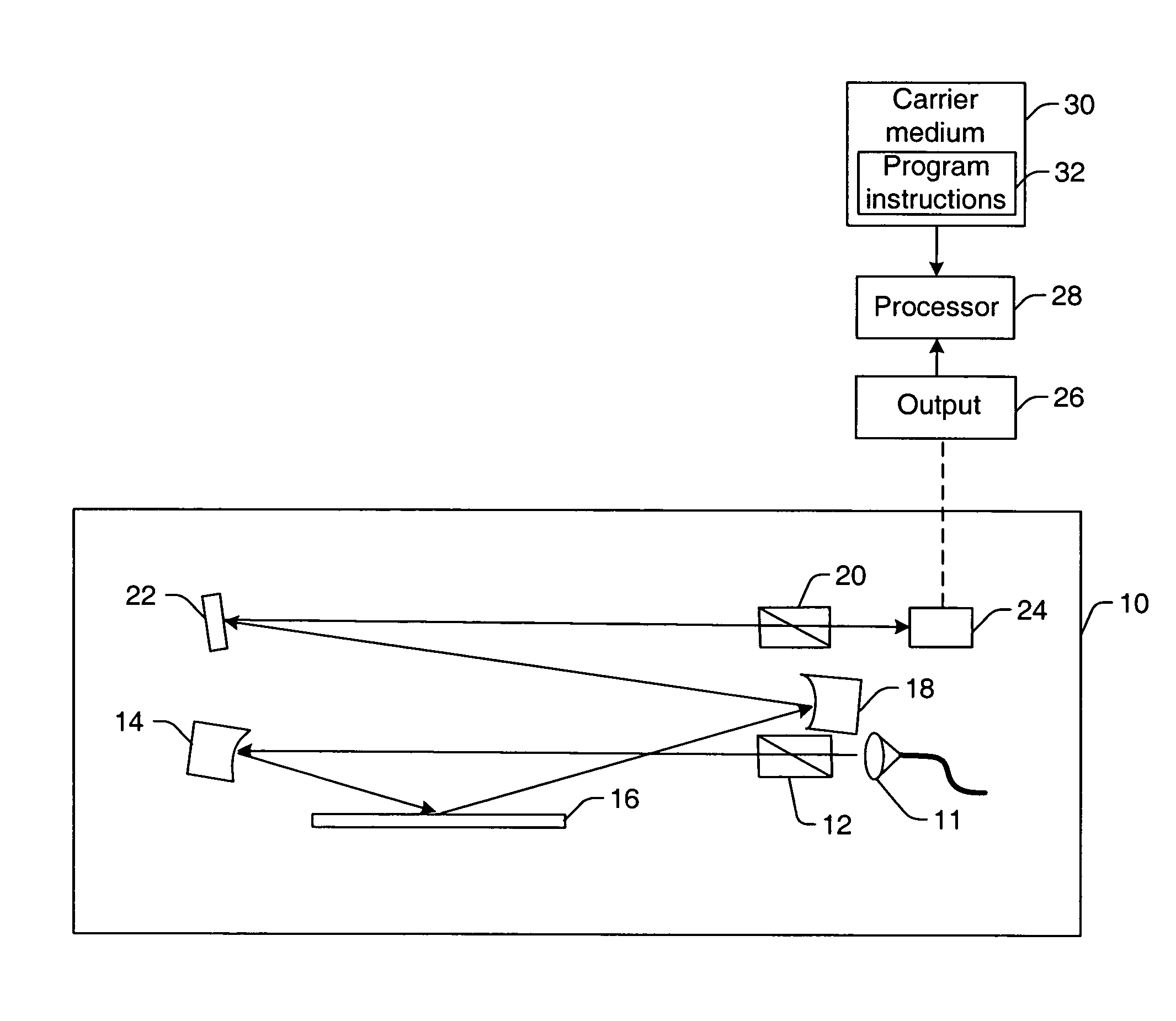
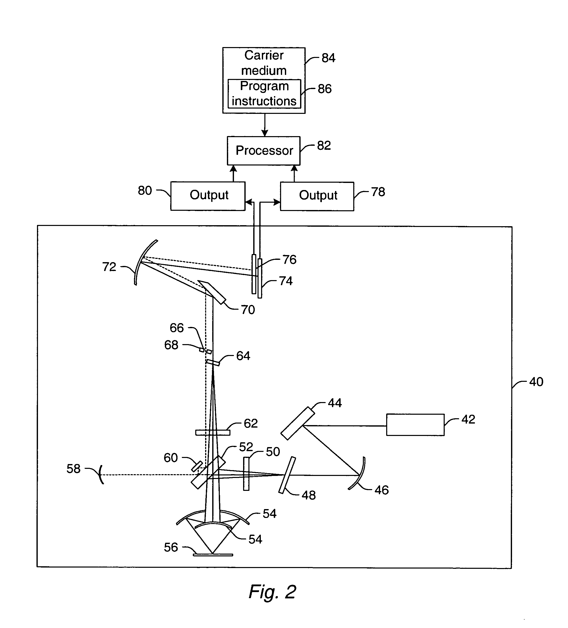
[0031]As used herein, the term “specimen” is generally defined as a wafer. The term “wafer” generally refers to substrates formed of a semiconductor or non-semiconductor material. Examples of such a semiconductor or non-semiconductor material include, but are not limited to, monocrystalline silicon, gallium arsenide, and indium phosphide. Such substrates may be commonly found and / or processed in semiconductor fabrication facilities.

[0032]A wafer may include only the substrate such as a virgin wafer. Alternatively, a wafer may include one or more layers formed upon a substrate. For example, such layers may include, but are not limited to, a resist, a dielectric material, and a conductive material. Examples of a dielectric material may include, but are not limited to, silicon dioxide, silicon nitride, silicon oxynitride, and titanium nitride. Additional examples of a dielectric material include “low-k” dielectric materials such as Black Diamond™ which is commercially available from Ap...


PUM


Abstract

Systems and methods for measuring stress in a specimen are provided. One system includes an optical subsystem configured to measure stress-induced birefringence in patterned structures formed on the specimen. In some embodiments, the optical subsystem may be configured as a spectroscopic ellipsometer, a multi-angle laser ellipsometer, a polarimeter, a polarized reflectometer, or some combination thereof. The system also includes a processor coupled to the optical subsystem. The processor is configured to determine stress in a material of the patterned structures using the stress-induced birefringence measurements. One method includes measuring stress-induced birefringence in patterned structures formed on the specimen using an optical technique. The method also includes determining stress in a material of the patterned structures using the stress-induced birefringence measurements.

Description

BACKGROUND OF THE INVENTION[0001]1. Field of the Invention[0002]The present invention generally relates to systems and methods for measuring stress in a specimen. Certain embodiments relate to methods that include determining stress in patterned structures on a specimen using stress-induced birefringence measurements of the patterned structures.[0003]2. Description of the Related Art[0004]The following description and examples are not admitted to be prior art by virtue of their inclusion in this section.[0005]Fabricating semiconductor devices such as logic and memory devices typically includes processing a substrate such as a semiconductor wafer using a number of semiconductor fabrication processes to form various features and multiple levels of the semiconductor devices. For example, lithography is a semiconductor fabrication process that involves transferring a pattern from a reticle to a resist arranged on a semiconductor wafer. Additional examples of semiconductor fabrication pr...

Claims


Application Information

Patent Timeline
IPC IPC(8): G01B11/16G01J4/00
CPCG01J3/021G01J3/0229G01J3/447G01J4/00G01L1/241H01L2924/0002G01N2203/0641H01L22/12H01L2924/00
Inventor JANIK, GARYKRISHNAN, SHANKAR
Owner KLA TENCOR TECH CORP
Why Eureka
Try Eureka