Triple cascode power amplifier of inner parallel configuration with dynamic gate bias technique

a power amplifier and cascode technology, applied in the direction of gated amplifiers, amplifiers with semiconductor devices only, amplifiers with semiconductor devices, etc., can solve the problems of low efficiency, difficult to design high-power amplifiers, and low breakdown voltage between gates and drains

Inactive Publication Date: 2007-10-02
ELECTRONICS & TELECOMM RES INST
View PDF6 Cites 65 Cited by
  • Summary
  • Abstract
  • Description
  • Claims
  • Application Information

AI Technical Summary

Benefits of technology

[0012]It is, therefore, an object of the present invention to provide a power amplifier which does not deteriorate characteristics of a high frequency, and can increase power gain and output power by solving a problem of a low breakdown voltage of a deep submicron transistor.
[0013]It is another object of the present invention to provide a power amplifier which does not deteriorate the input / output matching state and linearity, and can increase efficiency in a low power mode simultaneously.
[0016]The preferred embodiments of the present invention will be described in detail hereinafter with reference to the attached drawings so that those skilled in the art that the present invention is included can embody the technological concept and scope of the invention easily. Meanwhile, hereinafter, the same drawing code of described drawing codes is a same element performing a same function.

Problems solved by technology

However, the shorter the length of the CMOS transistor channel is, the thinner a gate silicon dioxide film of the transistor becomes, which causes a problem that a breakdown voltage (BV) between a gate and a drain is lowered.
This makes it difficult to design a high power amplifier.
To solve the problem, there has been an attempt to substitute the common gate transistor M2 with the input / output transistor, but efficiency is very low since it also generates a problem of deteriorated high frequency characteristic.
The lower the output of the amplifier is, the less efficient the linear power amplifier becomes.
As a result, the efficiency of the power amplifier is substantially degraded in a communication environment that the power amplifier should be used with a backoff in the range of 0 to 10 dB from its maximum output due to linearity.
This method decreasing DC power consumption by lowering the bias voltage increases the efficiency of the power amplifier in the low power mode, but it has a problem that as the bias voltage is lowered, the linearity gets worse.
Using the transmission line as an output matching circuit network is desirable in the respect that each mode can be independently operated, but it causes a problem that it is not easy to integrate the transmission line.
When an output matching circuit network is made of passive elements, it is difficult to isolate the power amplifiers 22 and 23 from each other, and the passive elements also decrease the output power and efficiency.
An additional matching circuit may be required to compensate the change of the input / output impedance, which reduces the output power and efficiency, and raises costs.

Method used


Image

  • Triple cascode power amplifier of inner parallel configuration with dynamic gate bias technique
  • Triple cascode power amplifier of inner parallel configuration with dynamic gate bias technique
  • Triple cascode power amplifier of inner parallel configuration with dynamic gate bias technique

Examples


first embodiment

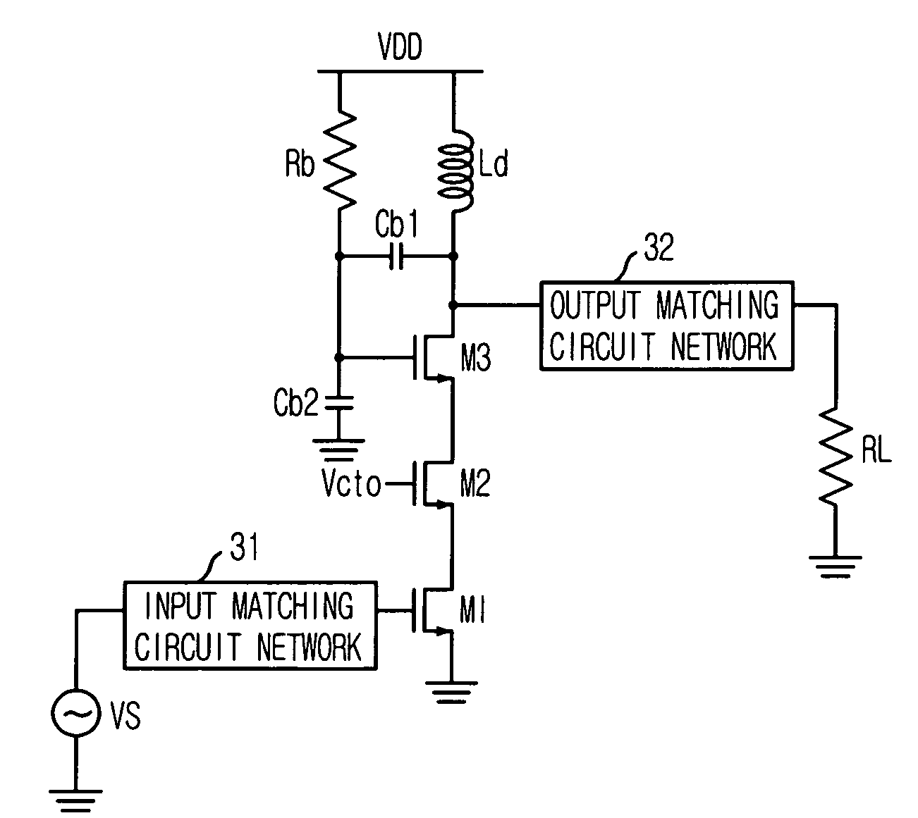
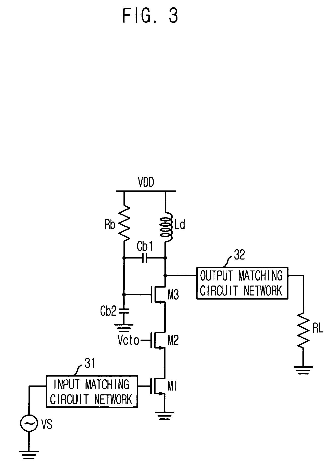
[0026]FIG. 3 is a circuit diagram showing a power amplifier in accordance with a first embodiment of the present invention.

[0027]As shown in FIG. 3, the power amplifier suggested in the first embodiment of the present invention has a triple cascode configuration including a dynamic gate bias by a voltage divider with capacitors Cb1 and Cb2. The triple cascode configuration is formed based on a serial connection of a common source transistor M1, a common gate transistor M2, and a transistor M3 with a dynamic gate bias.

[0028]The common source transistor M1, which is the first stage of the triple cascode configuration, is connected to ground at a source, connected to the source of the common gate transistor M2 at a drain, and connected to the input matching circuit network 31 at a gate. Considering the mentioned configuration, an input signal Vs impedance-matched through the input matching circuit network 31 is coupled to the gate of a common source transistor M1, amplified and outputt...

second embodiment

[0034]FIG. 4 is a circuit diagram describing the power amplifier suggested in the second embodiment of the present invention. It shows an example realizing a triple cascode power amplifier of the first embodiment in inner-parallel configuration.

[0035]As shown in FIG. 4, the power amplifier suggested in the second embodiment of the present invention has a configuration that three common gate transistors M2a to M2c and three common source transistors M1a to M1c are connected in parallel cascode configuration in addition to the configuration of the first embodiment. Herein, the number of the cascode branches, which are connected in parallel, is three, but the number is only for the sake of convenience in explanation and it can be varied properly.

[0036]The power amplifier of the second embodiment has a configuration for increasing efficiency in a low power mode while taking the advantages of the power amplifier of the first embodiment. In the configuration, cascode branches that three t...

third embodiment

[0054]FIG. 7 is a circuit diagram showing a power amplifier in accordance with a third embodiment of the present invention. Herein, the power amplifier having dynamic bias current and dynamic bias voltage in accordance with a third embodiment of the present invention is an example originated from the power amplifier in accordance with the second embodiment shown in FIG. 4.

[0055]As shown in FIG. 7, the power amplifier of the third embodiment further includes a detecting block 76 for detecting the amplitude of an input signal Vs in the power amplifier shown in FIG. 4 and a voltage providing block 73 for controlling an amplitude of DC supply voltage according to a control signal of the detecting block 76.

[0056]In the respect of a bias, a DC gate bias of the dynamic bias transistor M3 in the third stage is determined to be equal to a dynamic supply voltage and a dynamic gate bias according to the amplitude of an output signal is determined by a voltage divider of capacitors Cb1 and Cb2 ...


PUM


Abstract

Provided is a power amplifier which fits to a deep-submicron technology in radio frequency wireless communication. The power amplifier includes a cascode including a first transistor which receives and amplifies an input signal, and a second transistor which is connected to the first transistor in series and operated by a DC bias voltage; a third transistor which is connected between the cascode and an output end, operated by a dynamic gate bias and outputting a signal; and a voltage divider which includes first and second capacitors that are connected between the output end, i.e. a drain of the third transistor, and a ground in series, and provides the dynamic bias to a gate of the third transistor.

Description

FIELD OF THE INVENTION[0001]The present invention relates to a power amplifier; and, more particularly, to a power amplifier which fits to a deep-submicron technology in wireless communication based on a radio frequency.DESCRIPTION OF RELATED ART[0002]Rapid development of technologies makes it possible to produce diverse chips used for wireless communication at a low price by using a Complementary Metal Oxide Semiconductor (CMOS) process, and achieve almost the same performance compared with chips produced by using conventional III-V group compound semiconductor.[0003]Recent development of a CMOS manufacturing process makes the length of a channel of a CMOS transistor getting short. Accordingly, high frequency performance has been expected to be improved continuously. However, the shorter the length of the CMOS transistor channel is, the thinner a gate silicon dioxide film of the transistor becomes, which causes a problem that a breakdown voltage (BV) between a gate and a drain is l...

Claims


Application Information

Patent Timeline
Patent Type & Authority Patents(United States)
IPC IPC(8): H03F3/04
CPCH03F1/223H03F1/301H03F3/72H03F3/191H03F2203/7206H03F2200/27
Inventor OH, HYOUNG-SEOKYU, HYUN-KYUPARK, MUN-YANGKIM, CHEON-SOO
Owner ELECTRONICS & TELECOMM RES INST
Why Eureka
Try Eureka