Parametric profiling using optical spectroscopic systems

a technology of optical spectroscopic systems and parametric profiling, applied in the field of parametric profiling using optical spectroscopic systems, can solve the problems of insufficient measurement methods for a wide variety of very different profiles, method still has some drawbacks, and the fabrication of state-of-the-art devices requires a considerable number of process steps, so as to eliminate uncertainty, simplify the profile measurement of structures, and eliminate the effect of uncertainty

Inactive Publication Date: 2007-10-09
KLA TENCOR TECH CORP
View PDF44 Cites 70 Cited by
  • Summary
  • Abstract
  • Description
  • Claims
  • Application Information

AI Technical Summary

Benefits of technology

[0021]Where two diffracting structures are present on the same sample, or on different samples of the same lots made by the same processing steps, to simplify the profile measurement of the structures, the profile obtained from one diffracting structure may be used as the seed profile in an optimization process for determining the parameters of another diffracting structure.
[0022]Information obtained by a scatterometric measurement may be fed to a critical dimension-scanning electron microscope measurement (CD-SEM) on the same target, or a different target on the same wafer or on a different wafer in the same lot made by the same processing process. The use of scatterometric data would help eliminate uncertainty that exists in scanning electron microscope algorithms with respect to the wall angle dependence of critical dimension measurements, and provides an absolute calibration of the pitch for the scanning electron microscope elements.
[0023]Scatterometric measurement data may also be fed to an overlay measurement tool on the same target or a different target on the same wafer, or on a different wafer but in the same lot produced by the same process. The use of scatterometric data would assist in eliminating the uncertainty that would exist in overlay algorithms caused by the profiles of the target.
[0024]In some measurements, it may not be possible to obtain the properties of film stacks over and/or below the diffracting structure. In such event, it may be desirable to determin

Problems solved by technology

The fabrication of state-of-the-art devices requires a considerable number of process steps.
The current methods are inadequate for measuring a wide variety of very different profiles in the manufacturing process.
Furthermore, different sets of parameters, corresponding to different profiles, can produce indistinguishable spectroscopic data, resulting in a problem known as cross-correlation.
While the above-described method of Conrad et al. reduces the number of parameters that one needs to contend with, this method still has some drawbacks.
Thus, it cannot be used for measuring line profiles made of more than material, and for measuring optical parameters as well as geometric parameters.
None of the existing techniques has such capability.
However, in many situations the number of variables (e.g. underlying layer thickness in a damascene layer) is prohibitively larg

Method used


Image

  • Parametric profiling using optical spectroscopic systems
  • Parametric profiling using optical spectroscopic systems
  • Parametric profiling using optical spectroscopic systems

Examples


Embodiment Construction

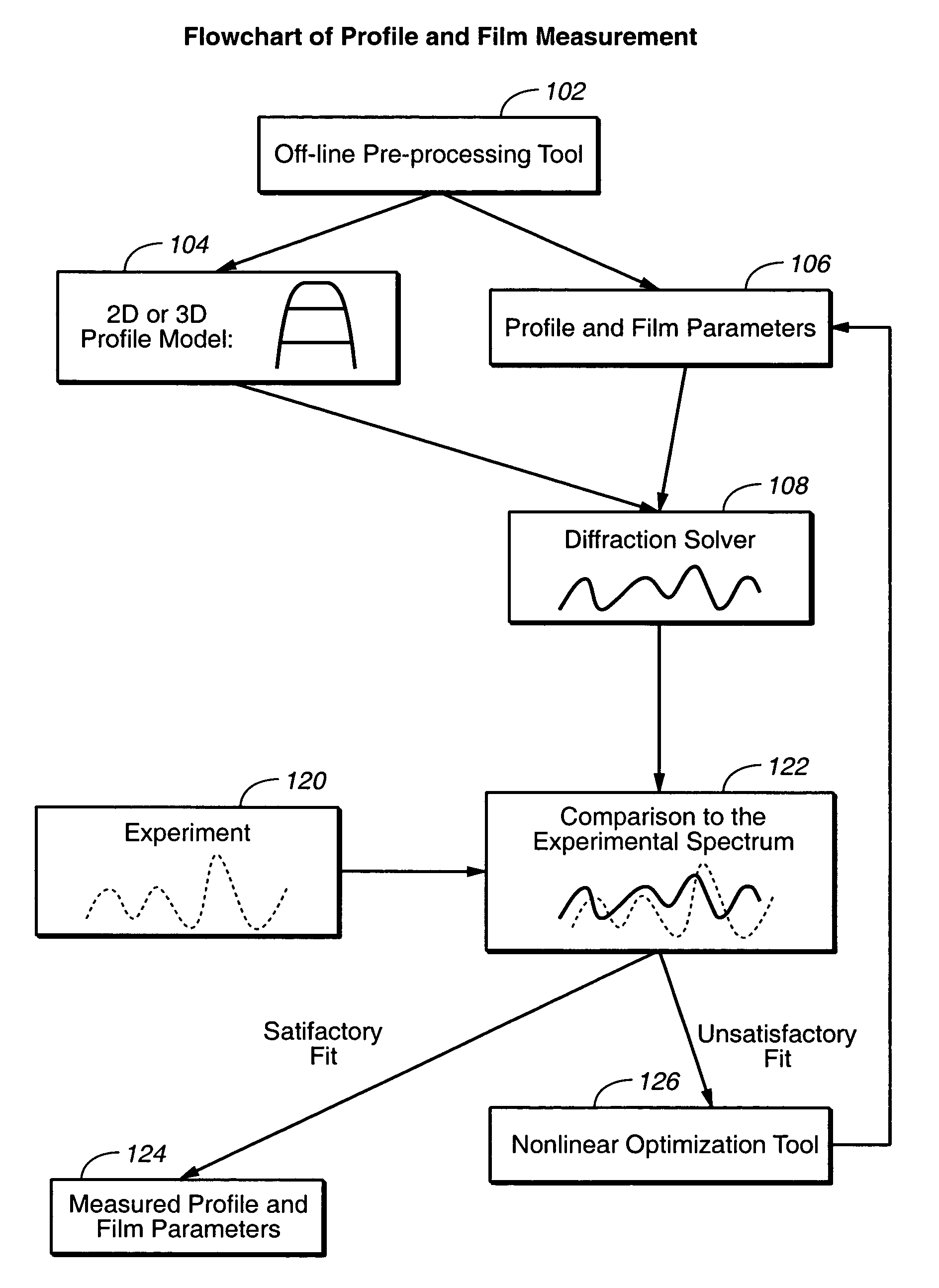
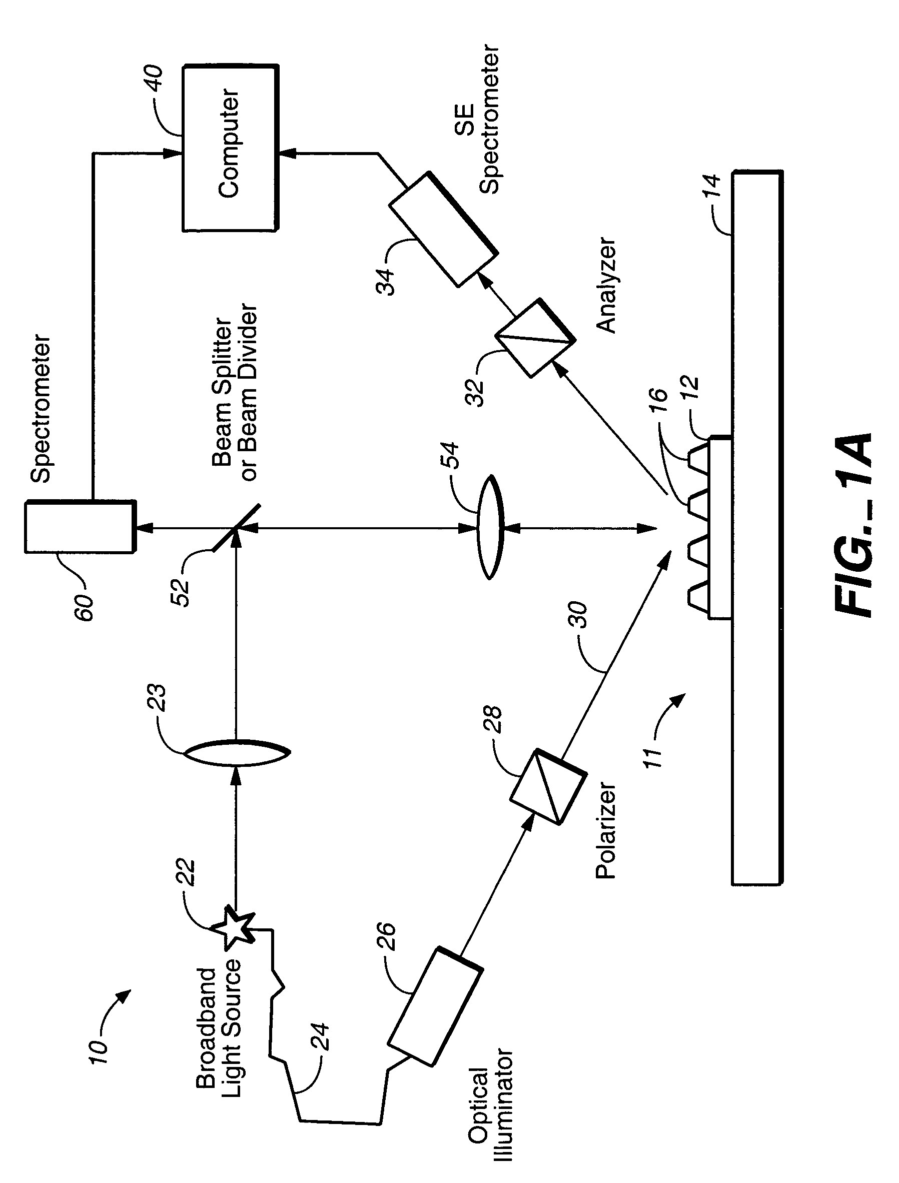
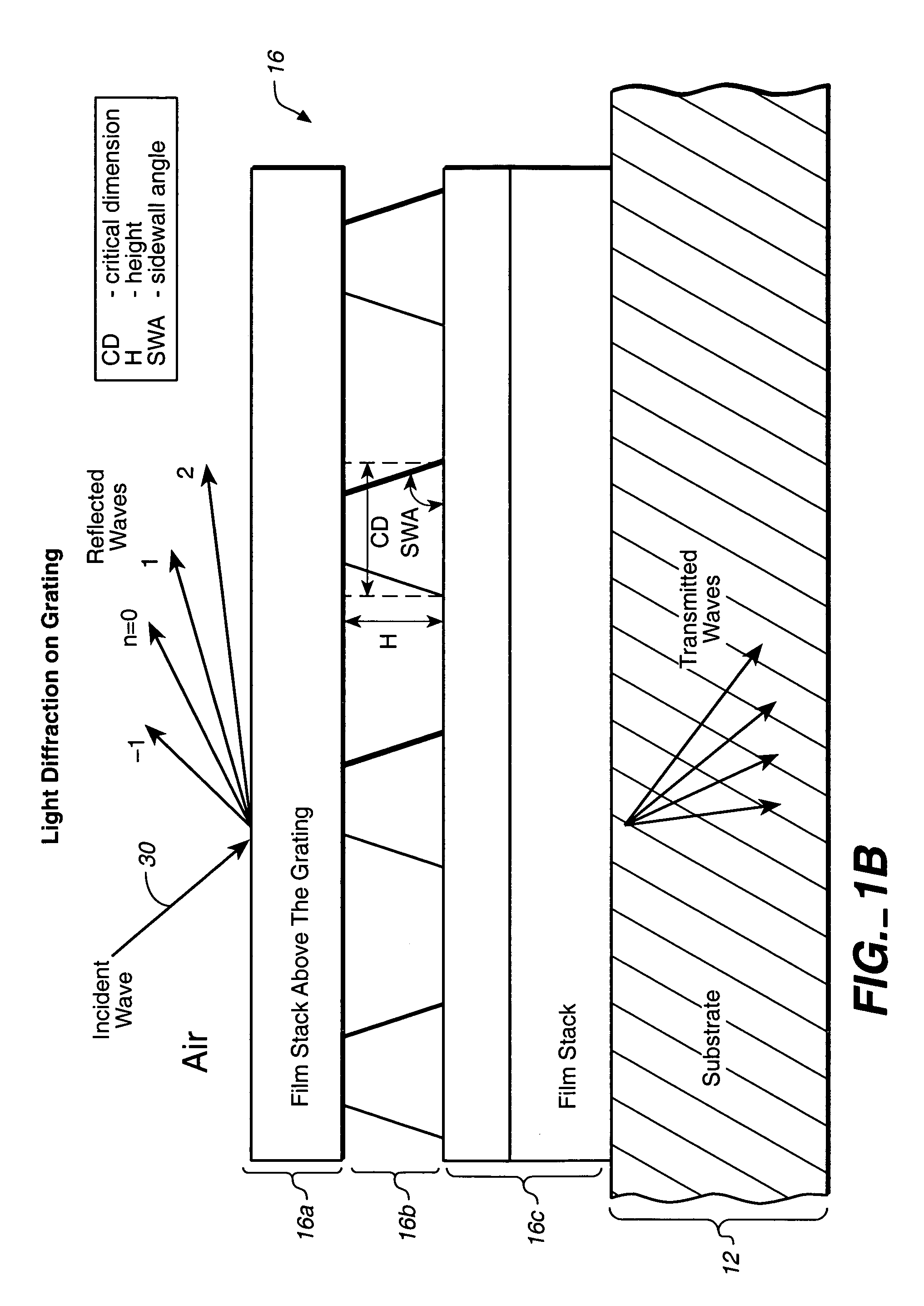
[0046]Even though much of the description below of algorithms and methods are described in terms of the reflected or transmitted intensities of the diffraction caused by the diffracting structure, it will be understood that the same techniques and algorithms may be used for data containing information concerning changes in the polarization state over different wavelengths (e.g. ellipsometric parameters Δ and Ψ as functions of wavelength). For this reason, it may be advantageous to employ an instrument which is capable of measuring both the reflected or transmitted intensities of the diffraction caused by the structure as well as changes in polarization state caused by the diffraction of the structure. A suitable system is described below in reference to FIG. 1A.

[0047]FIG. 1A is a schematic view of a spectroscopic diffraction-based metrology system to illustrate the preferred embodiment of the invention. As shown in FIG. 1A, system 10 may be used to measure reflected or transmitted i...


PUM


Abstract

A gallery of seed profiles is constructed and the initial parameter values associated with the profiles are selected using manufacturing process knowledge of semiconductor devices. Manufacturing process knowledge may also be used to select the best seed profile and the best set of initial parameter values as the starting point of an optimization process whereby data associated with parameter values of the profile predicted by a model is compared to measured data in order to arrive at values of the parameters. Film layers over or under the periodic structure may also be taken into account. Different radiation parameters such as the reflectivities Rs, Rp and ellipsometric parameters may be used in measuring the diffracting structures and the associated films. Some of the radiation parameters may be more sensitive to a change in the parameter value of the profile or of the films then other radiation parameters. One or more radiation parameters that are more sensitive to such changes may be selected in the above-described optimization process to arrive at a more accurate measurement. The above-described techniques may be supplied to a track/stepper and etcher to control the lithographic and etching processes in order to compensate for any errors in the profile parameters.

Description

CROSS REFERENCE TO RELATED APPLICATION[0001]This application is a non-provisional application and claims the benefit of Application No. 60 / 343,077, filed Dec. 19, 2001, which is incorporated herein by reference in its entirety.BACKGROUND OF THE INVENTION[0002]This invention relates in general to systems for finding profiles of topographical features of small dimensions, such as those of a diffracting grating, and in particular to such systems using optical spectroscopic techniques.[0003]As the integration density and speed of microelectronic devices increase, circuit structures continue to shrink in dimension size and to improve in terms of profile edge sharpness. The fabrication of state-of-the-art devices requires a considerable number of process steps. It is becoming increasingly important to have an accurate measurement of submicron linewidth and quantitative description of the profile of the etched structures on a pattern wafer at each process step. Furthermore, there is a grow...

Claims


Application Information

Patent Timeline
IPC IPC(8): G01B11/28G01N21/21G01N21/47G01N21/95G01N21/956G03F7/20
CPCG01N21/211G01N21/47G01N21/4788G01N21/9501G03F7/70641G01N21/95607G03F7/70616G03F7/70625G01N21/956G01N2021/213
Inventor SHCHEGROV, ANDREI V.FABRIKANT, ANATOLYNIKOONAHAD, MEHRDADLEVY, ADYWACK, DANIEL C.BAREKET, NOAHMIEHER, WALTERDZIURA, TED
Owner KLA TENCOR TECH CORP
Why Eureka
Try Eureka