

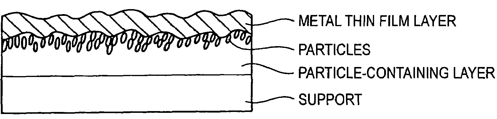
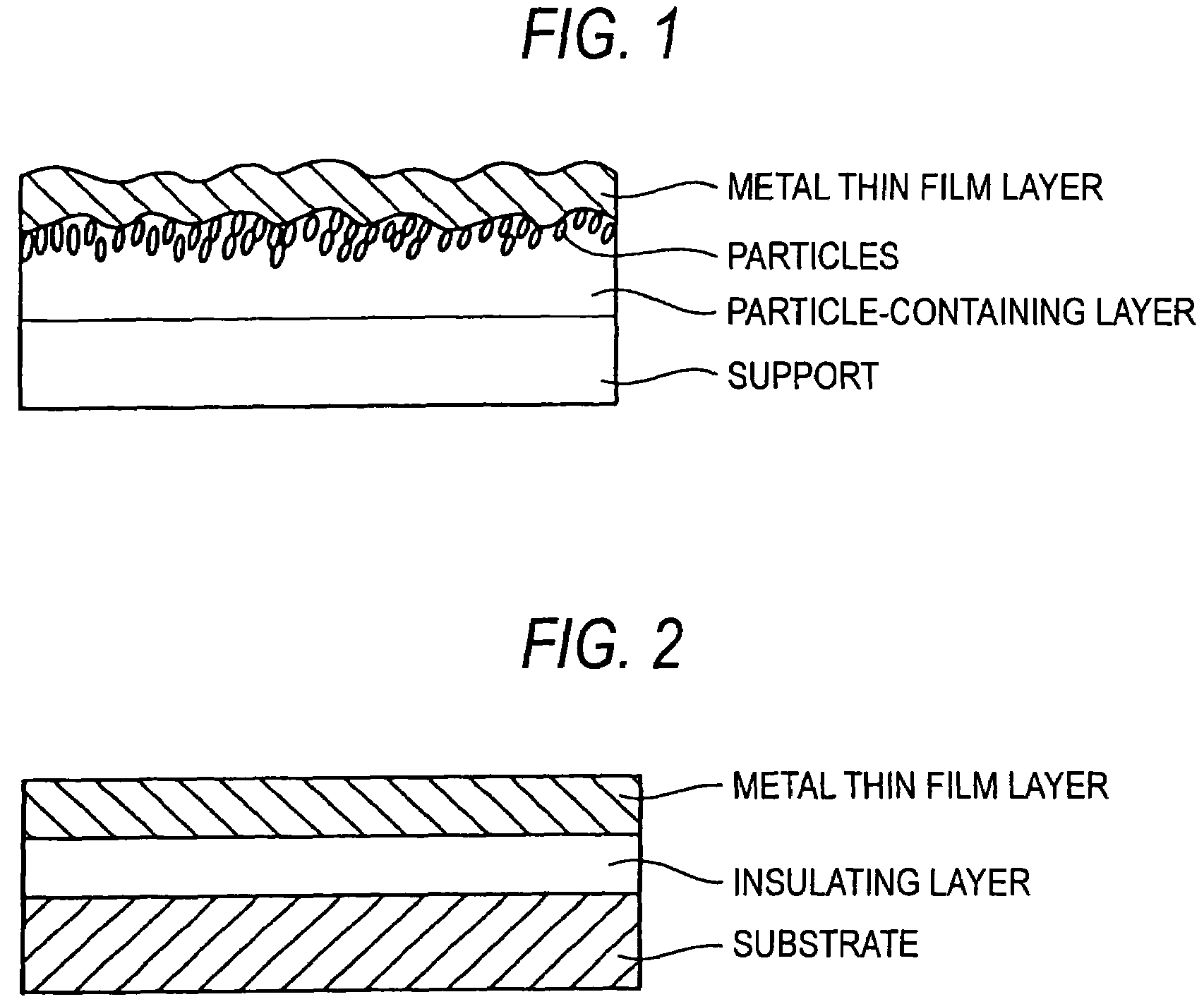
Conductive film and method for preparing the same
a technology of conductive film and conductive pattern, which is applied in the direction of superimposed coating process, liquid/solution decomposition chemical coating, conductive pattern formation, etc., can solve the problems of small via hole size, inconvenient to achieve high density, and the effect of high density
- Summary
- Abstract
- Description
- Claims
- Application Information
AI Technical Summary
Benefits of technology
Problems solved by technology
Method used
Image

Examples
example 1
[0094][Case 1] Preparation of Conductive Film 10-A:
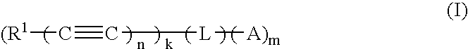
(1-1) Preparation of Metal Acetylide (Silver Salt of Illustrative Compound (1)):
[0095]A silver salt of the foregoing Illustrative Compound (1) shown as a specific example of the formula (I) was prepared in the following method.
[0096]16.4 g of sodium acetate and 16.7 g of silver nitrate were suspended in 200 mL of distilled water at 40° C. in the light-shielded state. 20.1 g of Illustrative Compound (1) was added dropwise to the suspension, and after stirring for 20 minutes, the mixture was cooled to room temperature. The reaction mixture was neutralized with 7.8 g of sodium hydrogencarbonate, and a supernatant was removed by decantation. Further, 200 mL of distilled water and 400 mL of chloroform were added for extraction. The chloroform layer was dried over anhydrous sodium sulfate, and the chloroform was distilled off in vacuo to obtain 29 g (substantially quantitatively) of a white wax-like solid. It was confirmed from NMR spectr...
example 2
Production of Single-Sided Copper-Plated Laminated Board and Evaluation of its Characteristics
[0134]Each of the five kinds of the conductive films 10-A, 20-B, 10-C and 20-D prepared in the foregoing Cases 1 to 4 and the conductive film E prepared in the foregoing Comparative Case 1 was cut into a size of 300 mm (MD)×300 (TD), and the surface of the copper foil layer side was placed on a glass fiber epoxy prepreg sheet (FR-4) having a thickness of 1 mm. The whole was sandwiched by two sheets of a smooth stainless steel plate and subjected to thermo-compression bonding at a temperature of 170° C. under a pressure of 50 kg / cm2 for 60 minutes. Next, the polyimide or polyethylene terephthalate as the support before the thermo-compression bonding was released using an adhesive sheet. With respect to the former four conductive films, the release interface was an interface between the support and the water-soluble resin layer. On the other hand, with respect to the conductive film E, releas...
example 3
Production of Double-Sided Copper-Plated Laminated Board
[0137]With respect to the four kinds of the conductive films 10-A, 20-B, 10-C and 20-D prepared in the foregoing Cases 1 to 4, the respective two sheets were cut into a size of 300 mm (MD)×300 (TD), and a glass fiberepoxy prepreg sheet (FR-4) having a thickness of 1 mm was sandwiched by the both surfaces of the copper foil layer sides. The whole was further sandwiched by two sheets of a smooth stainless steel plate from the outside and subjected to thermo-compression bonding at a temperature of 170° C. under a pressure of 50 kg / cm2 for 60 minutes in the same manner as in Example 2. Next, the polyimide or polyethylene terephthalate as the support before the thermo-compression bonding was released using an adhesive sheet, and the released interface was shower washed at 40° C. for 30 seconds using a 0.5% by weight sodium carbonate aqueous solution, thereby removing the water-soluble resin layer on the copper foil surface. The subs...
PUM
| Property | Measurement | Unit |
|---|---|---|
| mean particle size | aaaaa | aaaaa |
| heat resistant temperature | aaaaa | aaaaa |
| thickness | aaaaa | aaaaa |
Abstract
Description
Claims
Application Information