

Process for atomic layer deposition of metal films
- Summary
- Abstract
- Description
- Claims
- Application Information
AI Technical Summary
Benefits of technology
Problems solved by technology
Method used
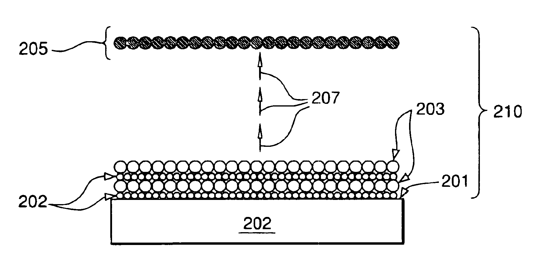
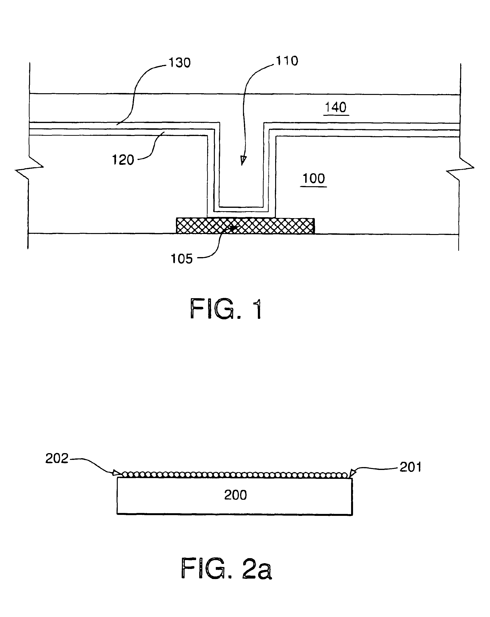
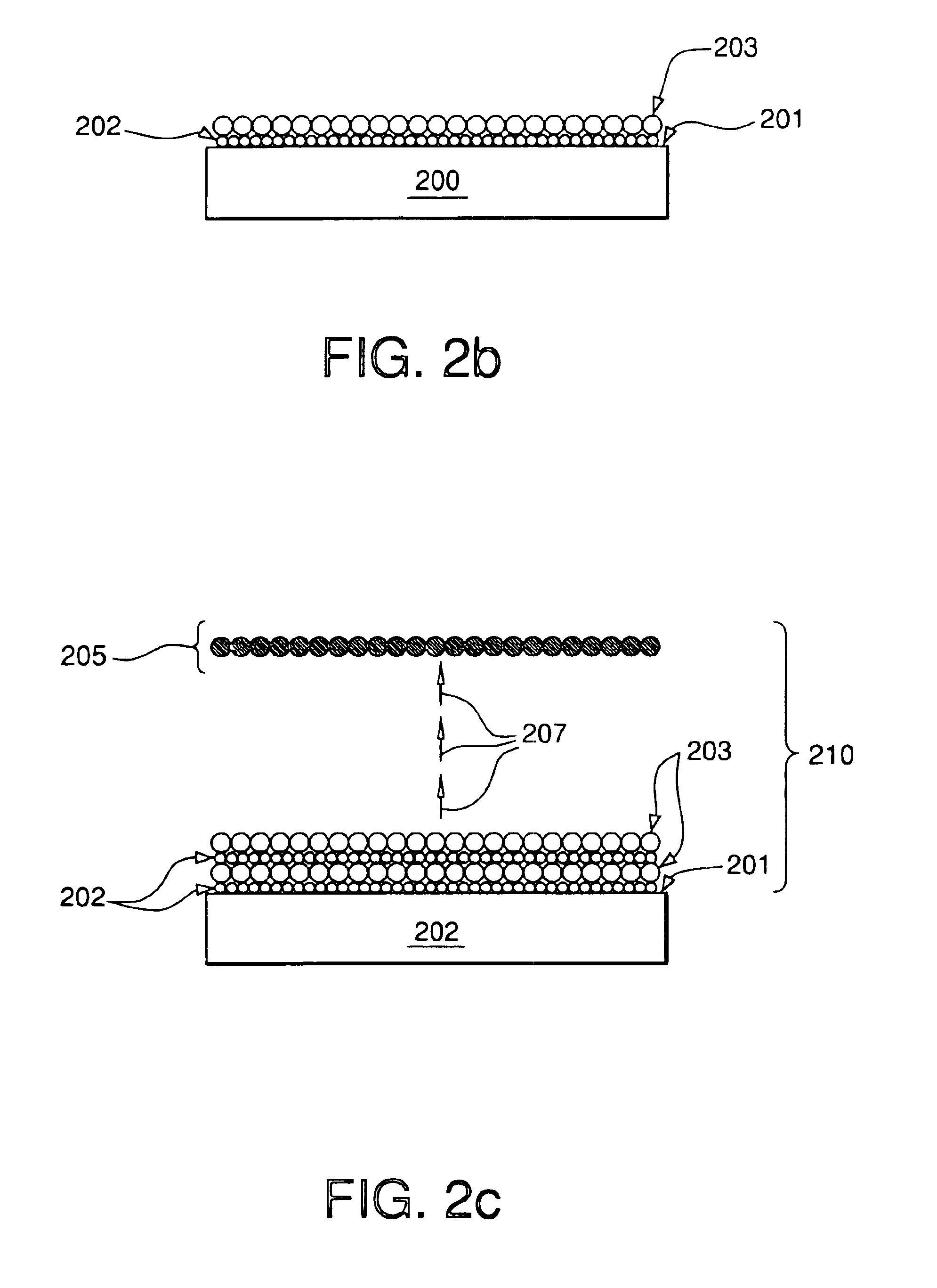
Image

Examples
example 1
is a solution-based model that illustrates that a copper-containing precursor such as Cu(I)(hfac)(tmvs) and a chloride-containing precursor such as HCl will react to form a copper chloride species which in turn can be reduced by a reducing agent such as diethylsilane to form a copper metal. It is anticipated that the copper based solid may not be entirely pure because it is precipitated out of solution as an insoluble inorganic salts and metals. Thus, the copper solid may contain traces of unreacted organic ligands. In the corresponding ALD experiment, or example 3, it is anticipated that the monolayer by monolayer chemical reactions are more likely to reach completion thereby achieving films of higher purity.
example 2
Treating [—CuNMe2SiMe2CH2CuNMe2SiMe2CH2—] Dissolved in THF with HCl
A 6.9 gram quantity of [—CuNMe2SiMe2CH2CuNMe2SiMe2CH2—], which was prepared in accordance with one of the methods disclosed in published U.S. Pat. Application 2002 / 0013487, was dissolved in an approximately 100 milliliter quantity of THF while stirring under a nitrogen atmosphere to provide a reaction mixture. A two molar equivalent amount of HCl (2.0 M in diethylether) was added to the reaction mixture at room temperature with stirring. The resulting reaction yielded a copper chloride precipitate sample, 3.02 gram and 78% of theoretical. The sample was filtered off and pumped dry.
Elemental analysis of the sample indicated that it contained 1.8 weight % carbon, 0.00 weight % hydrogen, and 0.91 weight % nitrogen. XRD measurements of the sample found it to contain pure copper chloride.
The sample was then treated with an excess quantity of diethylsilane at room temperature overnight to yield a copper colored solid. Elem...
example 3
ALD Preparation of Cu Films by Growing CuCl Film Using Cu(I)(hfac)(tmvs) and Hydrogen Chloride Followed by Diethylsilane Reduction
A 3″×0.5″ silicon wafer coated with a 200 Angstrom thick diffusion layer of TiN is placed into the chamber of ALD reactor comprised of a chamber fitted with a three-way mixing valve to permit the sequential purging of the chamber with halogen-containing precursor, nitrogen, and metal-containing precursor at atmospheric pressure. The wafer is held at a temperature of 25° C. A copper precursor, Cu(I)(hfac)(tmvs), is cooled to a temperature of 15° C. under a nitrogen atmosphere. Vapor from the copper precursor is introduced into the chamber at atmospheric pressure for a duration of 2 seconds and a flow rate of approximately 1800 standard cubic centimeters per minute (sccm). The chamber is then flushed with nitrogen gas for approximately 50 seconds at a flow rate of 1800 sccm to remove any residual Cu(I)(hfac)(tmvs) vapor. Vapor from a 0.5 M solution of anhyd...
PUM
 Abstract
Description
Claims
Application Information