Organic electroluminescent device

a technology of electroluminescent devices and organic el, which is applied in the direction of organic semiconductor devices, discharge tube luminescnet screens, other domestic articles, etc., can solve the problems of difficult even to bring the internal quantum efficiency close to 1, the current efficiency of the organic el device is not good, and the short circuit of the device can be prevented very effectively, and the yield or drive stability is excellen

Inactive Publication Date: 2007-11-06
SEMICON ENERGY LAB CO LTD
View PDF39 Cites 67 Cited by
  • Summary
  • Abstract
  • Description
  • Claims
  • Application Information

AI Technical Summary

Benefits of technology

[0037]At this time, in the organic EL device shown in FIGS. 1 and 2 can be designed such that the insulating layers are thickened sufficiently to prevent carrier injections respectively from the first and second electrodes. In this case, the organic EL device is

Problems solved by technology

However, there is means for applying large amounts of current to the organic material that is essentially insulators.
However, an organic EL device has a problem with respect to the current efficiency.
Therefore, in theory, it is possible to extract at most one photon from the recombination of one hole and one electron, and it is impossible to extract a plurality of photons therefrom.
However, in reality, it is difficult even to bring the internal quantum efficiency close to 1.
However, the range of material choice is unavoidably restricted since a phosphorescent material having high phosphorescent quantum efficiency φp should be used.
That is caused by that the organic compounds that can release phosphorescent light at r

Method used


Image

  • Organic electroluminescent device
  • Organic electroluminescent device
  • Organic electroluminescent device

Examples


embodiment 1

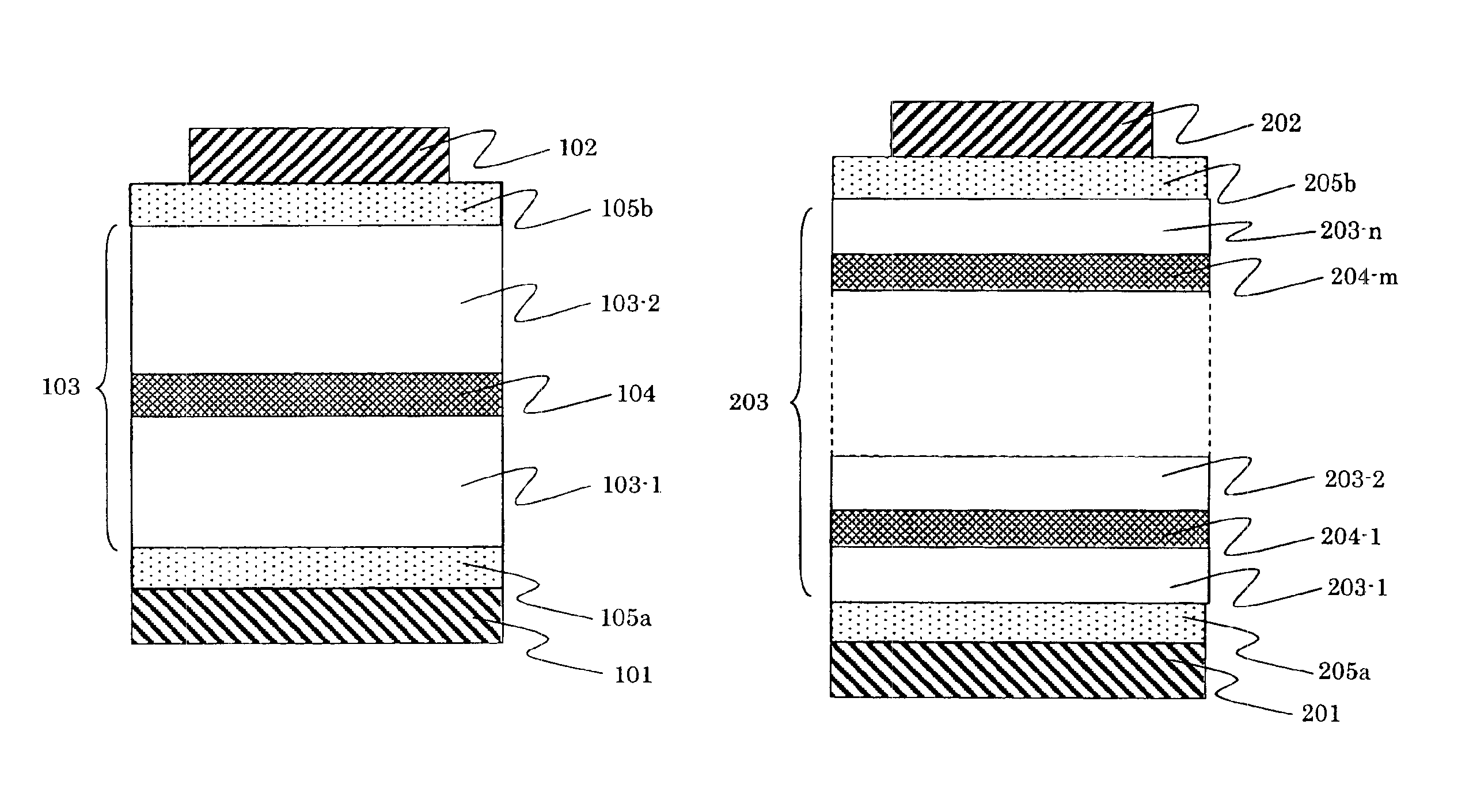
[0079]An organic EL device of the present invention that is fabricated by the vapor deposition will be specifically described in this embodiment. First, ITO is deposited to have a thickness of 100 nm as a first electrode on a glass substrate by vapor deposition, and oxide aluminum is deposited thereon to have a thickness of 300 nm as an insulating layer by EB vapor deposition.

[0080]Next, N,N′-bis(3-methylphenyl)-N,N′-diphenyl-benzidine (abbrev., TPD) as a hole transporting material and tris (8-quinolinolato) aluminum (abbrev., Alq) as an electron transporting material are co-deposited at 1:4 weight ratio to form a bipolar first electroluminescent layer to have a thickness of 100 nm. Here, 4-dicyanomethylene-2-methyl-6-(p-dimethylaminostyryl)-4H-pyran (abbrev., DCM) as a fluorescent pigment is doped to the center portion as much as 60 nm (between 20 to 80 nm from bottom of the thickness) to have weight ratio that TPD: Alq: DCM=1:4: 0.05.

[0081]After the first electroluminescent layer ...

embodiment 2

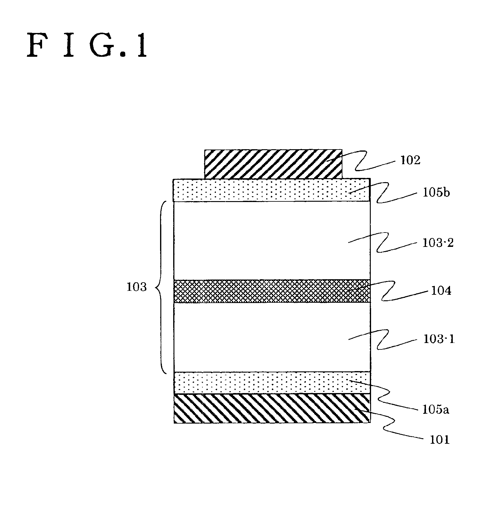
[0083]An organic EL device of the present invention fabricated by wet coating will be specifically described in this embodiment. First, poly(vinyl phenol) is coated by spin coating to have a thickness of 200 nm as an insulating layer on the glass substrate on which ITO is formed to have approximately 100 nm in thick as a first electrode. In addition, a material for solvent is isopropanol.

[0084]Second, poly(2-methoxy-5-(2-ethyl-hexoxy)-1,4-phenylenevinylene) (abbrev., MEH-PPV) is dissolved in dichloroethane, and coated 80 nm in thick by spin coating to form a first electroluminescent layer

[0085]After the first electroluminescent layer is formed in such a way, aqueous solution of poly(ethylene dioxythiophene) doped with polystyrene sulfonic acid (abbrev., PEDOT / PSS) is spin coated to form a bipolar carrier generation layer to have a thickness of 100 nm.

[0086]Thereafter, a second electroluminescent layer is continuously formed in exactly the same way as the first electroluminescent lay...

embodiment 3

[0087]An organic EL device of the present invention fabricated by coating with polymer composite films containing luminous pigments and bonding without using vapor deposition will be specifically described in this embodiment.

[0088]First, poly(vinyl phenol) is coated by spin coating to have a thickness of 200 nm as an insulating layer on the plastic substrate (polyester substrate or polyimide substrate) on which ITO is formed 100 nm in thick as a first electrode. In addition, a material for solvent is isopropanol.

[0089]Next, dichloromethane solution prepared from 50 wt % polycarbonate as binder, 29 wt % TPD as a hole transporting material, 20 wt % 2,5-bis(1-naphthyl)-1,3,4-oxadiazole (abbrev., BND) as an electron transporting material, 1.0 wt % coumarin 6 as a luminous pigment is spin coated on the insulating layer to form a first electroluminescent layer to have 100 nm in thick.

[0090]After the first electroluminescent layer is formed in such a way, polyaniline doped with camphor-10-...


PUM


Abstract

An organic electroluminescence device of the present invention adapts a new concept in its configuration to improve its efficiency in addition to obtain a high reliability and good yielding. The organic electroluminescent device having an electroluminescent film containing an organic material capable of causing an electroluminescence and being arranged between a first electrode and a second electrode, includes: a carrier generation layer, which is a floating electrode, is embodied in the electroluminescent film; an insulting film between the first electrode and the electroluminescent film, and an insulating film between the second electrode and the electroluminescent film, wherein the organic electroluminescent device is driven by an alternating current bias.

Description

BACKGROUND OF THE INVENTION[0001]1. Field of the Invention[0002]The present invention relates to an organic electroluminescent device, having an organic compound layer that generates light upon application of an electric field. More particularly, the present invention relates to an organic electroluminescent device that emits light using alternating current bias.[0003]2. Description of the Related Art[0004]Compared to inorganic compounds, organic compounds have more various material systems and possibilities for synthesizing organic materials to have advanced various functions through appropriate molecular design. Further, things made from the organic compound have characteristics of being flexible, and moreover, having workability by polymerization. In light of these advantages, in recent years, the technique of photonics and electronics employing functional organic materials have been attracted attention.[0005]The technique of photonics utilizing optical properties of organic mate...

Claims


Application Information

Patent Timeline
IPC IPC(8): H01J1/62H05B33/00H05B33/14H01L51/50H01L51/52
CPCH01L51/5012H01L51/5278H01L51/5096Y10S428/917H01L2251/564H10K50/13H10K50/11H10K50/18H10K50/17H10K50/19H10K71/841H10K50/81H10K50/805H10K50/82H10K50/84
Inventor TSUTSUI, TETSUO
Owner SEMICON ENERGY LAB CO LTD
Why Eureka
Try Eureka