Method of forming a photoresist pattern and method for patterning a layer using a photoresist

Active Publication Date: 2007-11-20
SAMSUNG ELECTRONICS CO LTD
View PDF11 Cites 5 Cited by
  • Summary
  • Abstract
  • Description
  • Claims
  • Application Information

AI Technical Summary

Benefits of technology

[0008]The present invention provides a method for forming a resist, and a method of patterning a layer using the resist pattern. The resist exhibits an improv

Problems solved by technology

This reduction in thickness of the resist layer undesirably deteriorates resistance to dry etching, and serious line edge roughness (LER) is often observed.
However, according to the BLR technique, adhesion to underlying layer materials is weak and solubility to a developer solution is relatively poor, making it difficult to achieve a high resolution.
However, this technique still has several limitations.
That is, it is quite difficult to adjust a CD bias

Method used


Image

  • Method of forming a photoresist pattern and method for patterning a layer using a photoresist
  • Method of forming a photoresist pattern and method for patterning a layer using a photoresist
  • Method of forming a photoresist pattern and method for patterning a layer using a photoresist

Examples


Example

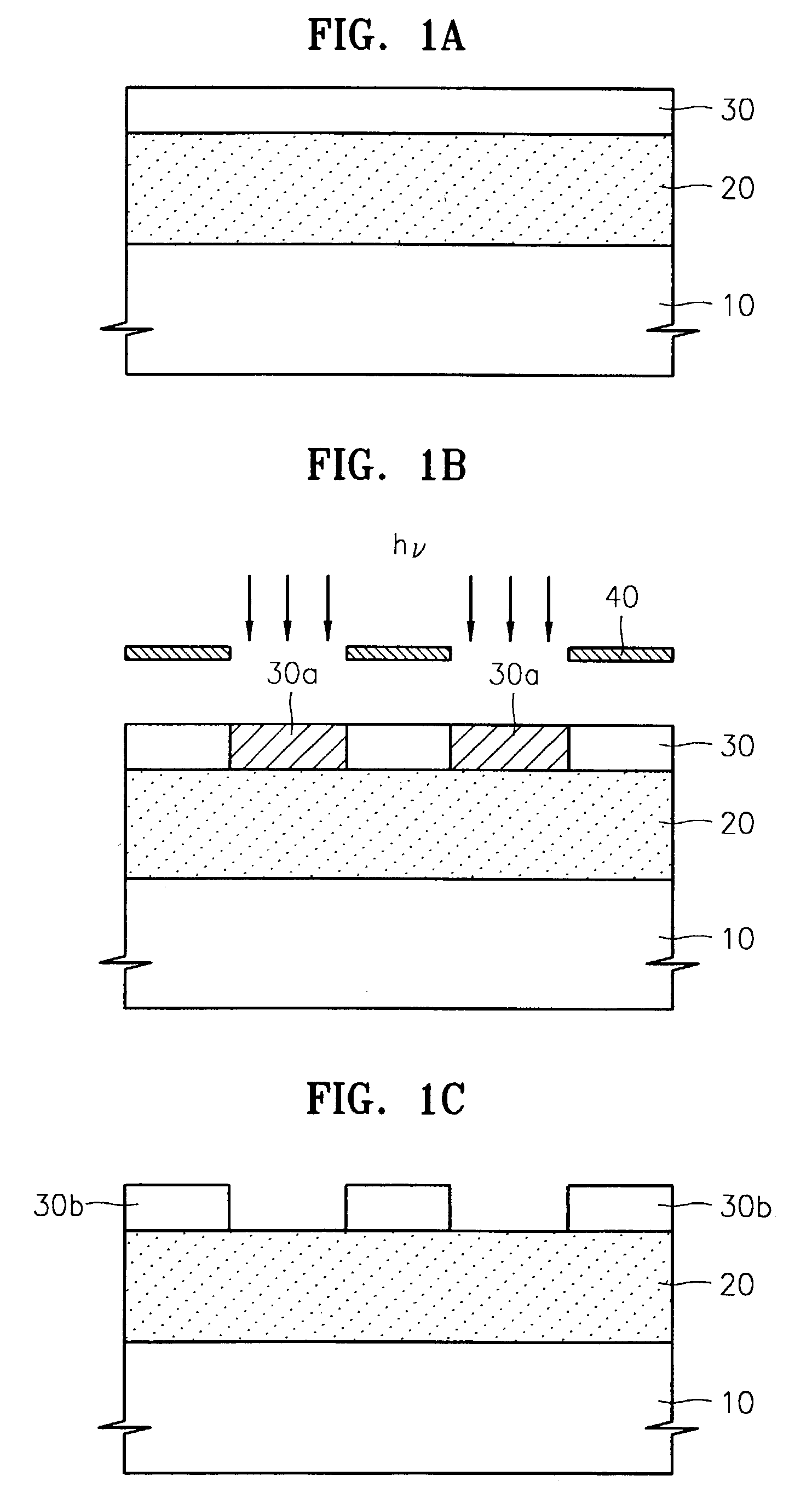
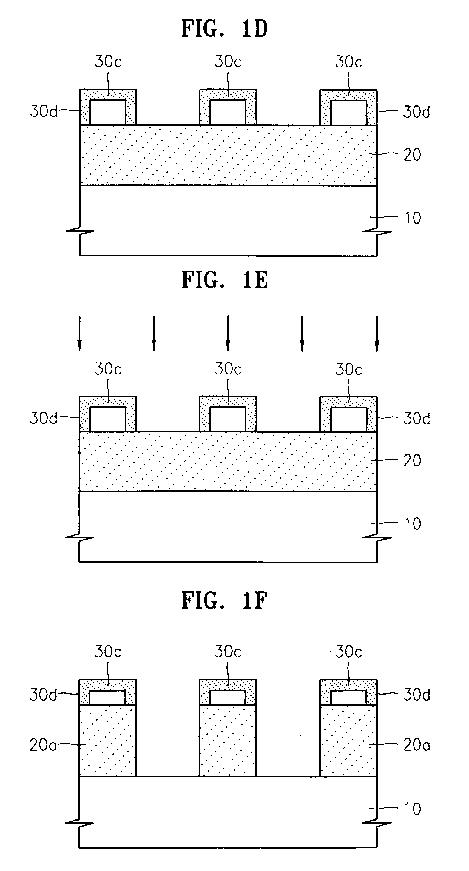
[0039]FIGS. 1A through 1F are cross-sectional views for explaining sequential process steps of a method for patterning a layer on a semiconductor substrate according to an embodiment of the present invention.

[0040]Referring to FIG. 1A, an organic anti-reflective coating (ARC) 20 is formed on a semiconductor substrate 10. The invention is not limited to any particular materials of the organic ARC 20, and conventional anti-reflective coating materials can be used. The organic ARC 20 may be formed to a thickness of approximately 0.02 to 1.0 μm.

[0041]Thereafter, a resist layer 30 is formed on the organic ARC 20, preferably to a thickness of approximately 0.1 to 1.0 μm. The resist layer 30 contains a photosensitive polymer having a hydroxy group, and can be formed of any material which is suitable for use in a photolithography process employing a desired light source, such as a KrF (248 nm) excimer laser, an ArF (193 nm) excimer laser, or a F2 (157 nm) excimer laser.

[0042]Preferably, the...


PUM

PropertyMeasurementUnit
Depthaaaaaaaaaa
Exposure limitaaaaaaaaaa
Photosensitivityaaaaaaaaaa

Abstract

An organic anti-reflective coating (ARC) is formed over a surface of a semiconductor substrate, and a resist layer including a photosensitive polymer is formed on the ARC. The photoresistive polymer contains a hydroxy group. The resist layer is then subjected to exposure and development to form a resist pattern. The resist pattern to then silylated to a given depth by exposing a surface of the resist pattern to a vapor phase organic silane mixture of a first organic silane compound having a functional group capable of reacting with the hydroxy group of the photoresistive polymer, and a second organic silane compound having two functional groups capable of reacting with the hydroxy group of the photoresistive polymer Then, the silylated resist pattern is thermally treated, and the organic ARC is an isotropically etched using the thermally treated resist pattern as an etching mask.

Description

BACKGROUND OF THE INVENTION[0001]1. Field of the Invention[0002]The present invention generally relates to lithography processes employed in semiconductor device fabrication and, more particularly, the present invention relates to the formation of a patterned photoresist, and to a method of a patterning a surface layer of a semiconductor substrate using a patterned photoresist.[0003]A claim of priority is made to Korean Patent Application No. 2002-0048129, filed Aug. 14, 2002, the contents of which are incorporated herein by reference in their entirety.[0004]2. Description of the Related Art[0005]As the integration density of semiconductor devices continues to increase and as chip sizes continue to decrease, there is an increasing need to form patterns with finer and finer dimensions. However, as the patterned dimensions in lateral directions are reduced as necessary to form fine patterns, it is also necessary to reduce the thickness of the photoresist layer in order to avoid the co...

Claims


Application Information

Patent Timeline
IPC IPC(8): G03F7/30G03F7/004H01L21/027G03F7/40
CPCG03F7/405Y10S430/108H01L21/027
Inventor LEE, SUNG-HOWOO, SANG-GYUNCHAE, YUN-SOOKKIM, JI-SOO
Owner SAMSUNG ELECTRONICS CO LTD
Why Eureka
Try Eureka