Conductive metal oxide gate ferroelectric memory transistor

a ferroelectric memory transistor and metal oxide gate technology, applied in semiconductor devices, digital storage, instruments, etc., can solve the problems of difficult to form a high-quality ferroelectric film directly on the silicon substrate, difficult to achieve effective transistor operation of the above mfs transistor, and difficult to achieve stable operation of the ferroelectric transistor. achieve the effect of reducing the operating voltage of the ferroelectric transistor

Inactive Publication Date: 2007-11-20
SHARP KK
View PDF33 Cites 8 Cited by
  • Summary
  • Abstract
  • Description
  • Claims
  • Application Information

AI Technical Summary

Benefits of technology

[0011]The present invention discloses a ferroelectric transistor having a conductive oxide in the place of the gate dielectric. By replacing the gate dielectric with a conductive oxide, the bottom gate of the ferroelectric layer is conductive through the conductive oxide to the silicon substrate, therefore there is no floating gate effect. The memory retention degradation related to the leakage current associated with the charges trapped within the floating gate is eliminated. Furthermore, the operating voltage for the ferroelectric transistor can be reduced to the ferroelectric layer programming voltage because of the absence of the gate dielectric.
[0014]The conductive oxide further can have the advantages of possible lattice matching with the ferroelectric layer, reducing or eliminating the oxygen diffusion problem at the ferroelectric interface to improve the reliability of the ferroelectric transistor, and possible etch selectivity improving with other dielectric and metal films.

Problems solved by technology

However, effective transistor operation of the above MFS transistor is difficult to achieve due to the requirement of the ferroelectric / silicon interface.
When a ferroelectric film is deposited directly on the silicon substrate, metals and oxygen from the ferroelectric layer may diffuse into the ferroelectric-silicon interface, creating interface trap charges, affecting the polarization of the ferroelectric film, and overall may make the operation of the ferroelectric transistor becoming unstable.
Further, since the thermal expansion coefficient and lattice structure of a ferroelectric film is not compatible with silicon, it is very difficult to form a high-quality ferroelectric film with a clean interface directly on the silicon substrate.
However, they incorporate other difficulties such as higher operation voltage and trapped charges in the bottom floating gate layer.
This additional resistor ensures that the potential of the floating gate will approach that of the source / drain region after a certain delay time, but this could affect the high speed switching characteristics of the ferroelectric memory.
In either designs, the higher operation voltage issue still remains due to the presence of the gate dielectric.

Method used


Image

  • Conductive metal oxide gate ferroelectric memory transistor
  • Conductive metal oxide gate ferroelectric memory transistor
  • Conductive metal oxide gate ferroelectric memory transistor

Examples


first embodiment

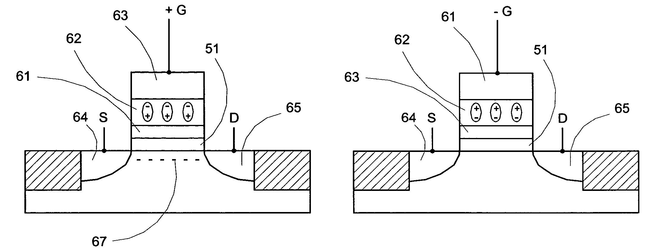
[0025]the present invention is shown in FIG. 3, illustrating an n-channel conductive oxide gate ferroelectric transistor. The gate stack of the present invention comprises a top gate electrode 63, a ferroelectric film 62, a bottom gate electrode 61 and a conductive oxide gate 51, positioning on a p-type silicon substrate 63, and disposed between the source 64 and drain 65 regions having a high concentration of n-type impurity ions. The ferroelectric transistor is isolated by the isolation trenches 66. The gate insulator of the present invention transistor is replaced with a conductive oxide such as InO2 or RuO2 to prevent floating gate effect.

[0026]FIG. 4 show the operation of the above n-channel conductive oxide ferroelectric transistor. In FIG. 4A, when a positive voltage is applied to the gate electrode 63, polarization of the ferroelectric film 62 occurs with electrons are pulled to the top and holes are pulled to the bottom of the ferroelectric film. Electrons are then accumula...

second embodiment

[0029]In the invention, the bottom gate electrode is omitted. Thus gate stack of the conductive oxide gate ferroelectric transistor comprises a top gate electrode 163, a ferroelectric film 162, and a conductive oxide gate 151 as shown in FIG. 5.

[0030]The conductive oxide in the present invention is preferably a conductive metal oxide, but can be a conductive oxide without any metal components. The conductive oxide can make good interface with the silicon substrate, and can be selected to have a good lattice matching with the deposited ferroelectric film, especially ones having perovskite crystal structures.

[0031]Furthermore, a conductive oxide serving as electrodes for the ferroelectric film may improve the quality of the ferroelectric film, and thus the operation of the ferroelectric transistor. A ferroelectric film is generally formed in an oxidizing ambience such as a deposition process with oxygen as a reactive gas, or an annealing process in an oxygen ambience to improve the st...


PUM


Abstract

The present invention discloses a ferroelectric transistor having a conductive oxide in the place of the gate dielectric. The conductive oxide gate ferroelectric transistor can have a three-layer metal / ferroelectric / metal or a two-layer metal / ferroelectric on top of the conductive oxide gate. By replacing the gate dielectric with a conductive oxide, the bottom gate of the ferroelectric layer is conductive through the conductive oxide to the silicon substrate, thus minimizing the floating gate effect. The memory retention degradation related to the leakage current associated with the charges trapped within the floating gate is eliminated. The fabrication of the ferroelectric transistor by a gate etching process or a replacement gate process is also disclosed.

Description

FIELD OF THE INVENTION[0001]This invention related generally to semiconductor device and nonvolatile memory transistor, and more particularly to ferroelectric gate transistor structures and methods of fabrication.BACKGROUND OF THE INVENTION[0002]Ferroelectric materials are composed of many randomly-distributed permanently polarized regions. When an electric field is applied, the regions with a polarization component in the direction of the electric field grow at the expense of the non-aligned regions so that a net polarization can result. If the electric field decreases, the polarization also decreases but at a slower rate so that even when the electric field becomes zero, a remnant polarization remains. A negative coercive field is required to bring the polarization to zero. This hysteresis behavior of a ferroelectric material is the basis of ferroelectric nonvolatile memory devices.[0003]Currently there are two types of ferroelectric nonvolatile memory devices: ferroelectric capac...

Claims


Application Information

Patent Timeline
Patent Type & Authority Patents(United States)
IPC IPC(8): H01L21/331H01L21/335H01L27/105G11C11/22H01L21/28H01L21/336H01L21/8246H01L29/78
CPCG11C11/22H01L21/28273H01L21/28291H01L29/78391H01L29/66553H01L29/66825H01L29/6684H01L29/66545H01L29/40111H01L29/40114
Inventor HSU, SHENG TENGLI, TINGKAI
Owner SHARP KK
Why Eureka
Try Eureka