
Preparation of CIGS-based solar cells using a buffered electrodeposition bath

a technology of cigs and solar cells, applied in photovoltaic energy generation, semiconductor devices, coatings, etc., can solve the problems of dwindling availability no ideal material that may be used to capture sunlight's broad energy spectrum, and high cost of silicon-based solar cells

Inactive Publication Date: 2007-11-20
DAVIS JOSEPH & NEGLEY
View PDF11 Cites 44 Cited by
  • Summary
  • Abstract
  • Description
  • Claims
  • Application Information

AI Technical Summary

Benefits of technology

[0009]Accordingly, it is a general object of the present invention to provide an improved process for the simultaneous electro-deposition of copper-indium-gallium-diselenide thin films to be used in the fabrication of photovoltaic solar cells.
[0010]Another object of the present invention is to provide a chemical bath that stabilizes the electro-deposition process and minimizes the production of metal oxides or hydroxide precipitates.
[0012]Still another object of the present invention is to provide an electro-deposition process that effectively utilizes source materials and minimizes waste generation.
[0013]Another object of the present invention is to provide a low cost electro-deposition process that produces highly efficient copper-indium-gallium-diselenide thin films that are efficient and have low-cost.
[0016]The present invention provides an inexpensive method of fabricating efficient copper-indium-gallium-diselenide (CIGS) thin films. According to one method of the present invention, a copper, indium, gallium, diselenide film layer is simultaneously deposited on a substrate by electro-deposition, wherein the substrate is placed within a buffered electro-deposition bath. The buffered bath allows for more uniform and consistent gallium deposition.

Problems solved by technology

Furthermore, there is no one ideal material that may be used to capture energy from the sunlight's broad energy spectrum.
Silicon-based solar cells are expensive because a large amount of raw material is required and the necessity to remove impurities and defects from the silicon.
Furthermore, advancements in the use of crystalline silicon in solar cells has resulted in an increasing demand for solar grade silicon, yet the availability of such silicon is dwindling.
A drawback of this process is selenium-containing gas such as H2Se is highly toxic and presents a great health risk to humans in large scale production environments.
Methods such as PVD of single crystals and polycrystalline films yield highly efficient solar cells, but PVD is very expensive and difficult to scale up for large scale production.

Method used


Image

  • Preparation of CIGS-based solar cells using a buffered electrodeposition bath
  • Preparation of CIGS-based solar cells using a buffered electrodeposition bath
  • Preparation of CIGS-based solar cells using a buffered electrodeposition bath

Examples


example 1

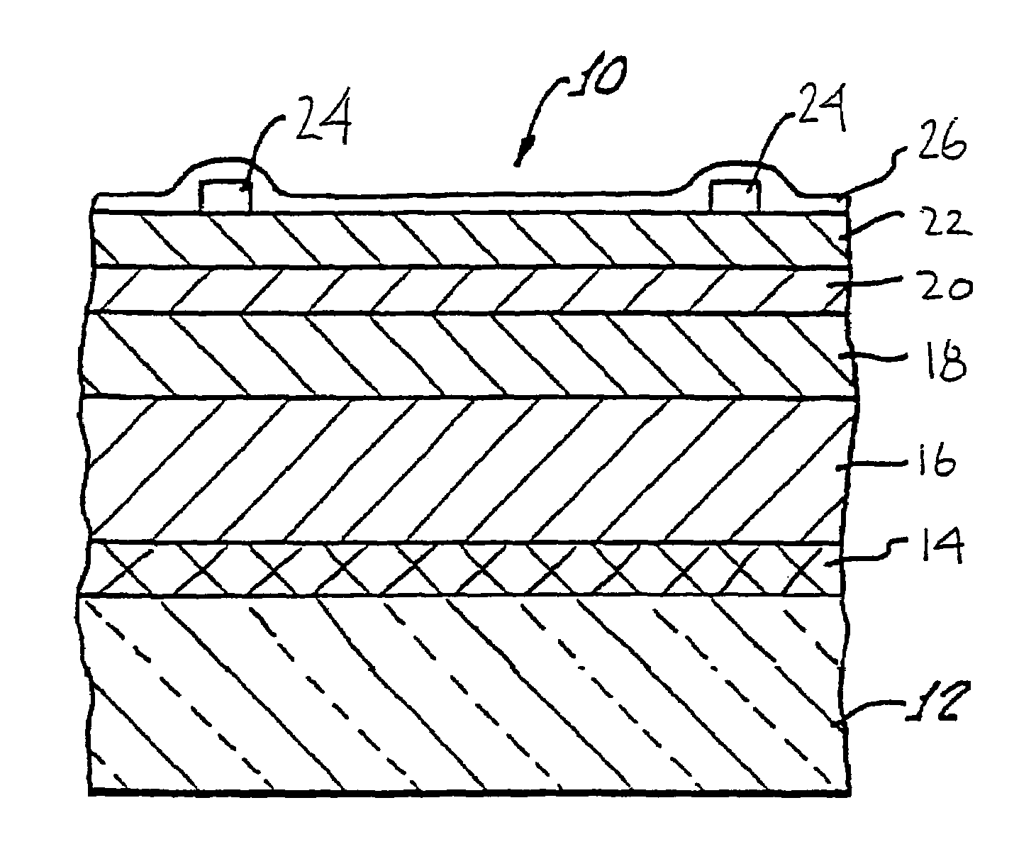
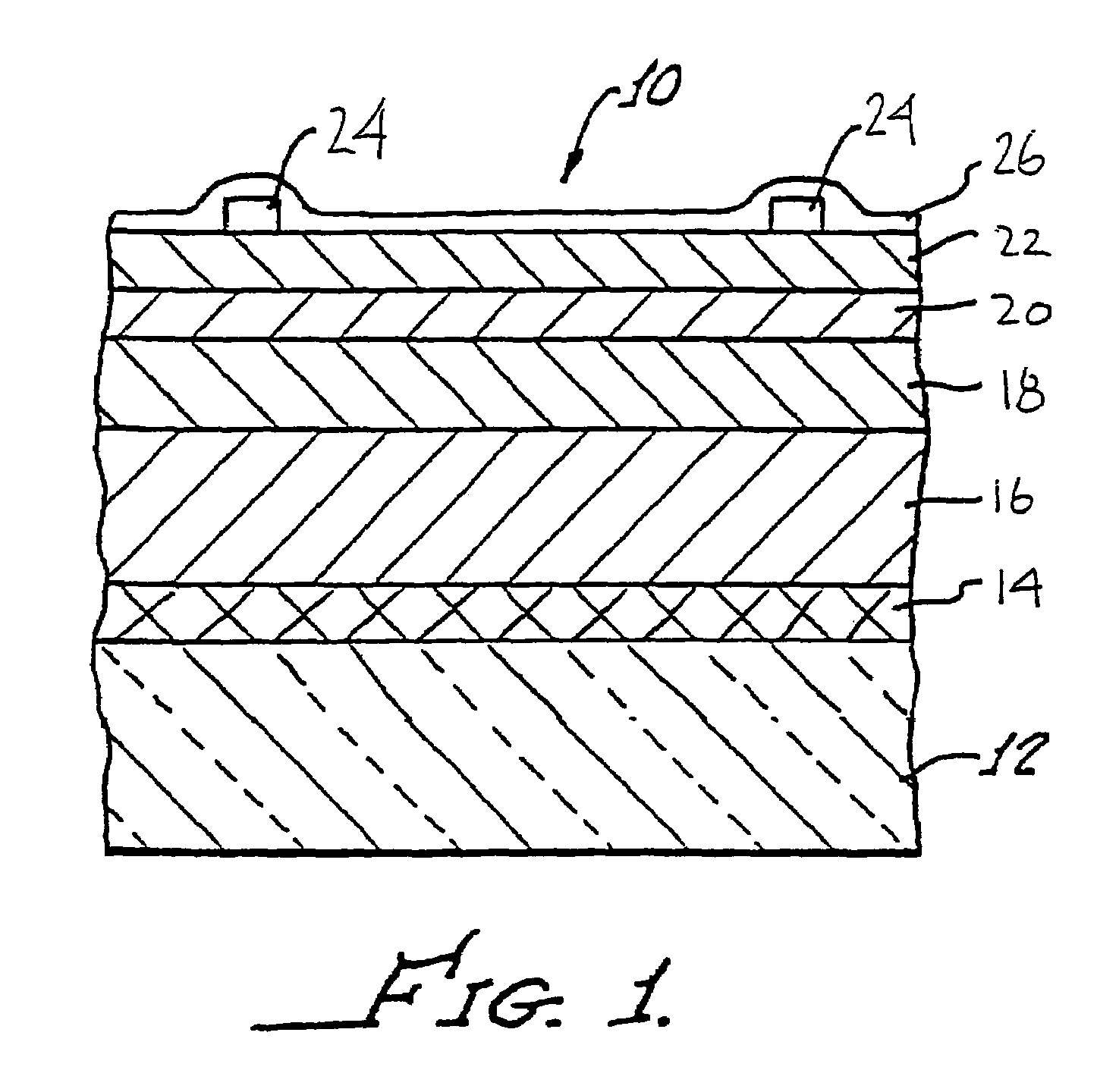
[0034]A thin film having a precursor layer comprised of copper-indium-gallium-selenium was deposited onto a glass substrate having molybdenum layer deposited thereon. The thin film layer was obtained by electro-deposition. The electro-deposition bath is prepared by adding 10 gm of pHydrion™ buffers (Aldrich, St. Louis, Mo., catalog #23,901-1), which contains potassium biphthalate and sulphamic acid, was dissolved in 800 ml water. A solution having 0.6 gm CuCl2, 1 gm InCl3, 0.8 gm GaCl3, 1 gm H2SeO3, and 10 gm LiCl was dissolved in 200 ml water. The metal ion solution and buffer solution were then mixed together. A three electrode system was used to deposit the precursor layer on the glass / Mo substrate wherein the glass / Mo substrate was used as the working electrode, platinum gauze was used as the counter electrode, and platinum was used as the pseudo-reference electrode. The electro-deposition voltage was at least 0.5 V. More particularly, a DC voltage of 0.9 V was applied for appro...

example 2

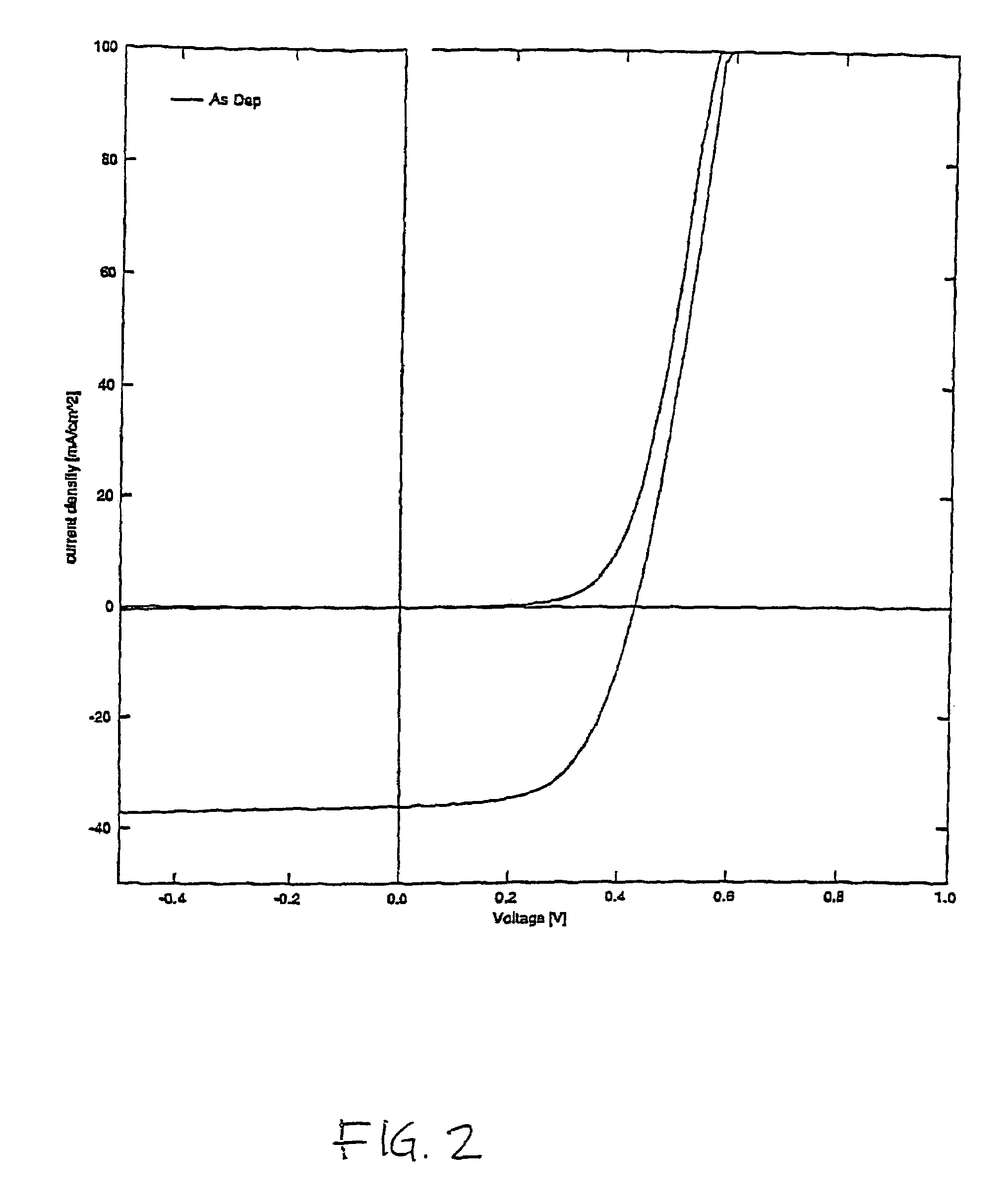
[0037]A photovoltaic cell was prepared according to Example 1, however 2400 Angstroms of indium was added in the PVD step. FIG. 3 shows the current density versus voltage of the finished cell having a 2400 Angstrom indium layer. The photovoltaic cell exhibited an overall efficiency of 9.02%. Other performance parameters for this cell are listed in Table 1 below.

[0038]

TABLE 1JcFill FactorTotal AreaExampleArea (cm2)Voc (mV)(mA / cm2)(%)Efficiency10.430.42936.0458.379.0220.430.44133.7565.289.72


PUM

PropertyMeasurementUnit
Fractionaaaaaaaaaa
Fractionaaaaaaaaaa
Electric potential / voltageaaaaaaaaaa

Abstract

A photovoltaic cell exhibiting an overall conversion efficiency of at least 9.0% is prepared from a copper-indium-gallium-diselenide thin film. The thin film is prepared by simultaneously electroplating copper, indium, gallium, and selenium onto a substrate using a buffered electro-deposition bath. The electrodeposition is followed by adding indium to adjust the final stoichiometry of the thin film.

Description

RELATED APPLICATIONS[0001]This application is a continuation of patent application Ser. No. 09 / 829,730 filed Apr. 10, 2001, now abandoned which claims the benefit of U.S. Provisional Patent Application Ser. No. 60 / 195,956, filed Apr. 10, 2000, and whose entire contents are hereby incorporated by reference.REFERENCE TO GOVERNMENT[0002]This invention was made with Government support under NREL-WFO-1326, Prime contract No. DE-AC36-83CH10093 awarded by the Department of Energy. The Government has certain rights in this invention.FIELD OF INVENTION[0003]The present invention relates to preparation of thin film photovoltaic solar cells. More particularly, the present invention relates to the fabrication of photovoltaic thin film by the simultaneous electro-deposition of copper, indium, gallium, and selenium onto a substrate.BACKGROUND OF THE INVENTION[0004]The most important components of photovoltaic cells are the semiconductor layers. The semiconductor layers are where sunlight is conve...

Claims


Application Information

Patent Timeline
IPC IPC(8): H01L31/00C25D5/00H01L21/00H01L31/032H01L31/0336
CPCH01L31/0322H01L31/0749Y02E10/541
Inventor BHATTACHARYA, RAGHU NATH
Owner DAVIS JOSEPH & NEGLEY
Learn More