Light emitting apparatus and method of manufacturing the same

Inactive Publication Date: 2007-11-27
SEMICON ENERGY LAB CO LTD
View PDF31 Cites 40 Cited by
  • Summary
  • Abstract
  • Description
  • Claims
  • Application Information

AI Technical Summary

Benefits of technology

[0010]The present invention has been made to solve the above problems, and therefore an object of the present invention is to provide a light emitting apparatus which reduces the wiring resistance of an electrically conductive film which forms the electrodes of light emitting elements, to thereby improve the uniformity of an image quality of the ligh

Problems solved by technology

However, there is a voltage drop (also called “IR drop”) due to a wiring resistance as a phenomenon which is a problem on the EL light emitting apparatus of the current drive type.
This problem is remarkable particularly in the case where the wiring length becomes long, and it is one of obstacles in enlarging a screen of the EL light emitting apparatus.
In particular, in the passive matrix EL light emitting apparatus, a transparent electrically conductive oxide film gene

Method used


Image

  • Light emitting apparatus and method of manufacturing the same
  • Light emitting apparatus and method of manufacturing the same
  • Light emitting apparatus and method of manufacturing the same

Examples


first embodiment

[0041]A light emitting apparatus in accordance with an embodiment of the present invention will be described with reference to FIG. 2. A pixel portion 202 is formed on a substrate 201 on which light emitting elements are formed. On the pixel portion 202, a scanning line (in this example, laminate wirings including anodes and auxiliary wirings) group 203 and a data line (in this example, cathodes) group 204 cross so as to be orthogonal to each other. On portions where the scanning line group 203 and the data line group 204 cross each other (hereinafter referred to as “cross portions”), EL elements where EL materials are interposed between the scanning lines and the data lines are formed. In this example, the pixel portion 202 is a pixel portion having a structure shown in FIG. 1.

[0042]In a region surrounding (in the exterior of) the pixel portion 202, an IC where a drive circuit that transmits the respective signals to the pixel portion 202 is formed is mounting through a Chip On Gla...

second embodiment

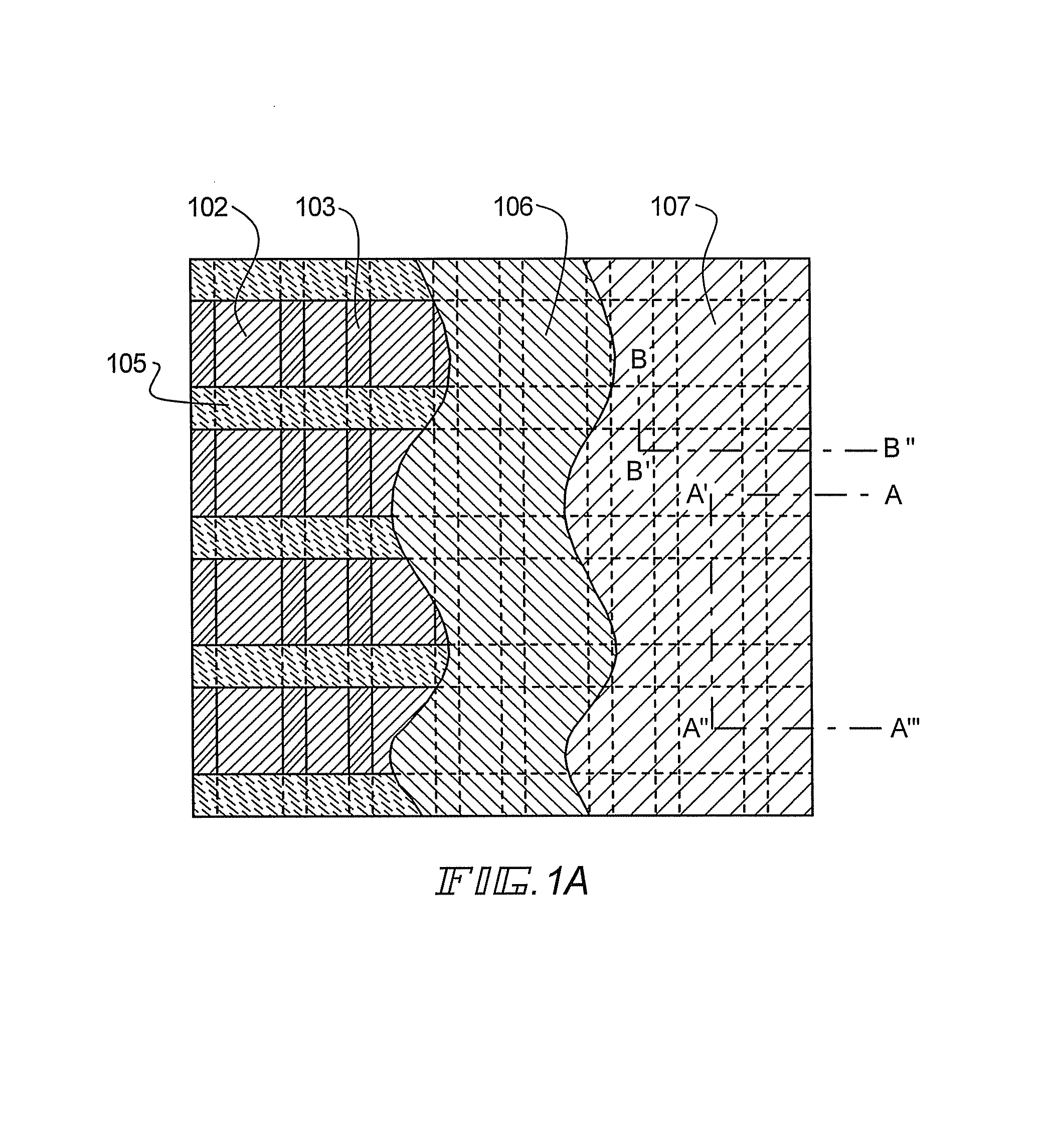
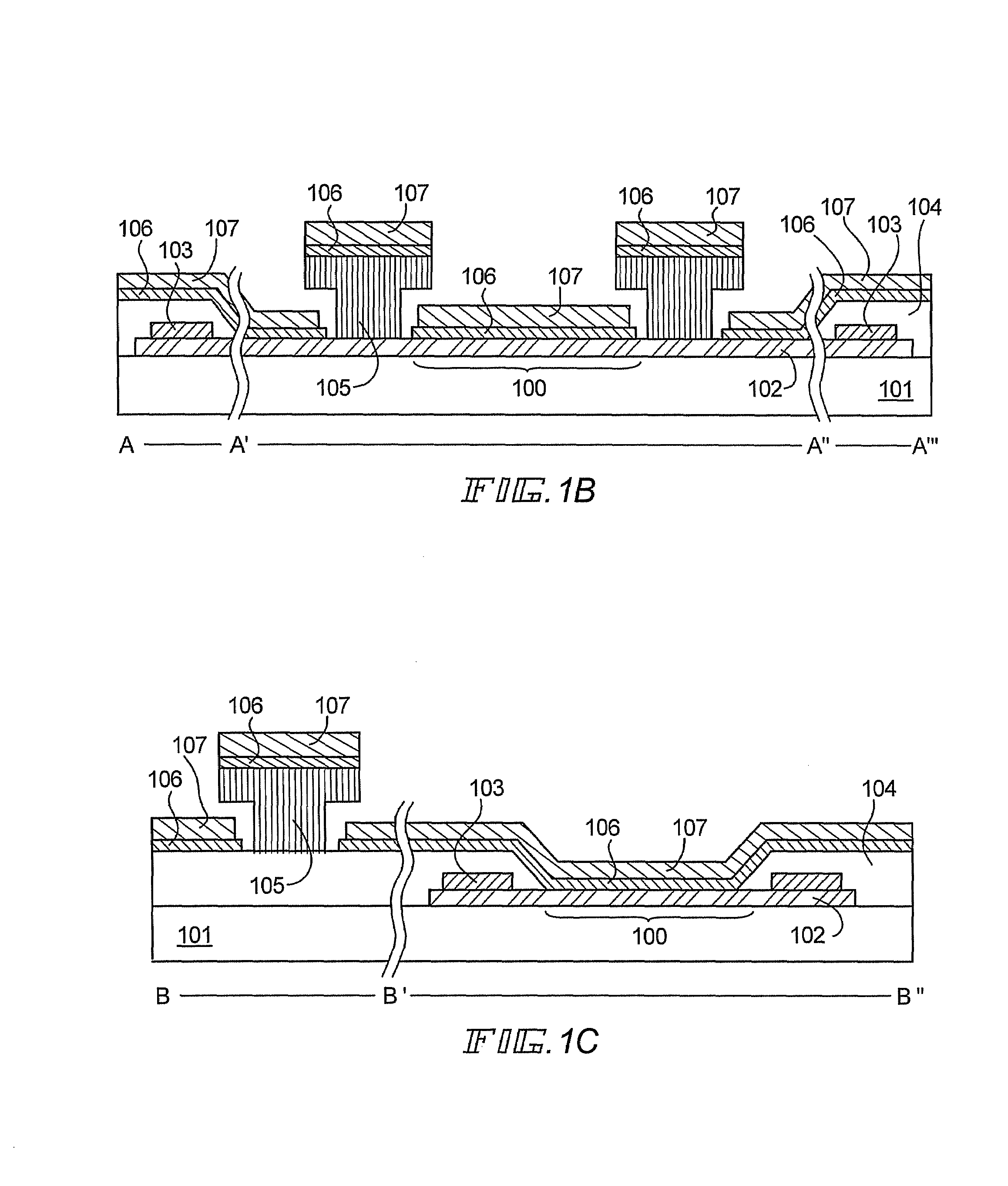
[0052]A light emitting apparatus according to another embodiment of the present invention will be described with reference to FIGS. 5A, 5B and 5C. FIG. 5A is a top view showing a light emitting apparatus according to the present invention, and FIG. 5B is a cross-sectional view taken along a line A-A′ in FIG. 5A. First, the top view of FIG. 5A will be described.

[0053]Referring to FIG. 5A, reference numeral 501 denotes a substrate which is made of a plastic material in this example. Polyimide, polyamide, acrylic resin, epoxy resin, PES (polyethylene sulfite), PC (polycarbonate), PET (polyethylene terephthalate) or PEN (polyethylene nafphthalate) as the plastic material may be made in a plate or a film so as to be used as the substrate 501.

[0054]Reference numeral 502 denotes scanning lines (anodes) formed of electrically conductive oxide films, and an electrically conductive oxide film where gallium oxide is added to zinc oxide is used in this embodiment. Nickel wirings 503 are dispose...

third embodiment

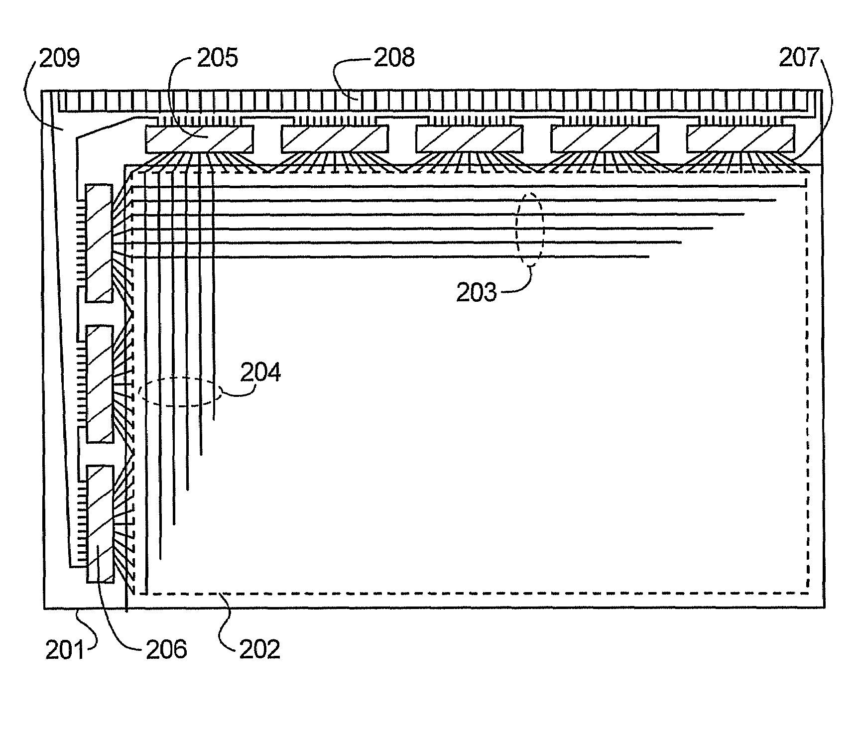
[0069]A circuit structure of the light emitting apparatus in accordance with an embodiment of the present invention will be shown in FIG. 6. A pixel portion 601 is formed with a plurality of scanning lines and a plurality of data lines, where a plurality of EL elements are formed. In a region surrounding the pixel portion 601, there are disposed a scanning line side driver 602 and a data line side driver 603, and stick drivers are used for those drivers (driver circuits). The structures of the stick drivers are identical with those described with reference to FIGS. 3 and 4.

[0070]Those stick drivers are connected to the input terminals 604. On a substrate where the pixel portion 601 is thus formed, there are formed the scanning line side driver 602, the data line side driver 603 and the input terminals 604.

[0071]Also, among a power supply circuit 608 including a control circuit 606, a stabilizing power supply 607 and an operational amplifier, the control circuit 606 and the power sup...


PUM


Abstract

A light emitting apparatus with high homogeneity in image quality is provided, which includes anodes 102 on an insulator 101, cathodes 107 orthogonal to the anodes 102, and EL layers 106 interposed between the anodes 102 and the cathodes 107, and auxiliary wirings 103 are electrically connected to the anodes 102. The auxiliary wirings 103 are made of a material lower in resistance than that of the anodes 102, thereby being capable of reducing the wiring resistance of the anodes 102.

Description

BACKGROUND OF THE INVENTION[0001]1. Field of the Invention[0002]The present invention relates to an apparatus (hereinafter referred to as “light emitting apparatus”) having an element where a luminescent material is interposed between a pair of electrodes (hereinafter referred to as “luminescent element”). In particular, the present invention relates to a light emitting apparatus (hereinafter referred to as “EL light emitting apparatus”) having a luminescent element (hereinafter referred to as “EL element”) which utilizes a luminescent material (hereinafter referred to as “EL material”) by which EL (electro luminescence) is obtained as the luminescent material. An organic EL display and an organic light emitting diode (OLED: organic light emitting diode) is contained in the light emitting apparatus according to the present invention.[0003]Also, the EL material which can be used in the present invention includes all of the luminescent materials that emit a light (phosphorescence and / ...

Claims


Application Information

Patent Timeline
IPC IPC(8): H01J1/62H01J63/04G09G3/30H01L27/32H01L51/52H05B33/06H05B33/26
CPCH01L27/3281H05B33/26H05B33/06H01L51/5212G09G3/30H10K59/17H10K50/814
Inventor YAMAZAKI, SHUNPEIFUKUNAGA, TAKESHI
Owner SEMICON ENERGY LAB CO LTD
Why Eureka
Try Eureka