Memory device having a nanocrystal charge storage region and method

a memory device and nanocrystal technology, applied in the field of memory devices, can solve the problems of large variation in the size distribution of nanocrystals, the device is not able to retain stored data or instructions when the device is turned, and the memory device is a volatile devi

Active Publication Date: 2007-12-18
ADVANCED MICRO DEVICES INC
View PDF18 Cites 23 Cited by
  • Summary
  • Abstract
  • Description
  • Claims
  • Application Information

AI Technical Summary

Problems solved by technology

A volatile memory device, on the other hand, does not retain the stored data or instructions when the device is turned off.
A drawback with this procedure is that the agglomeration process is random, thus there is a large variation in the size distribution of the nanocrystals.
In addition, the mean size of the nanocrystal is sensitive to the local temperature and metal film thickness, making it difficult to control their size distribution on large diameter semiconductor wafers.
Another drawback is that disposing the control oxide layer on the nanocrystals oxidizes them thereby degrading their charge storage capacities.
Other drawbacks of using the agglomeration process include the cost and complexity of using metals such as gold, platinum silicide, silver, and nickel to form the thin metal layer and the inability of the control oxide to sufficiently fill the spaces between small dimension nanocrystals.

Method used


Image

  • Memory device having a nanocrystal charge storage region and method
  • Memory device having a nanocrystal charge storage region and method
  • Memory device having a nanocrystal charge storage region and method

Examples


Embodiment Construction

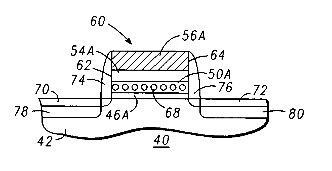
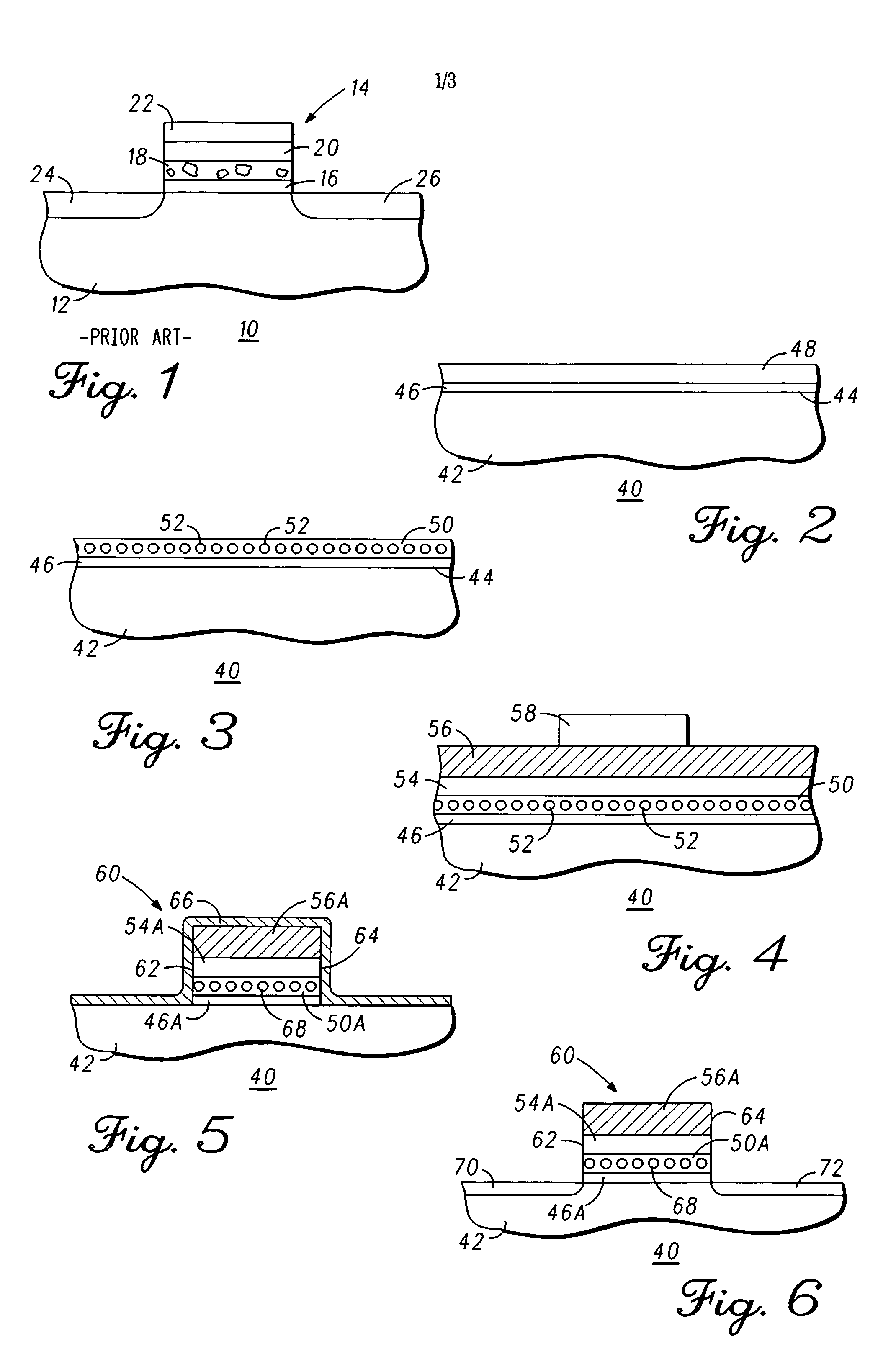
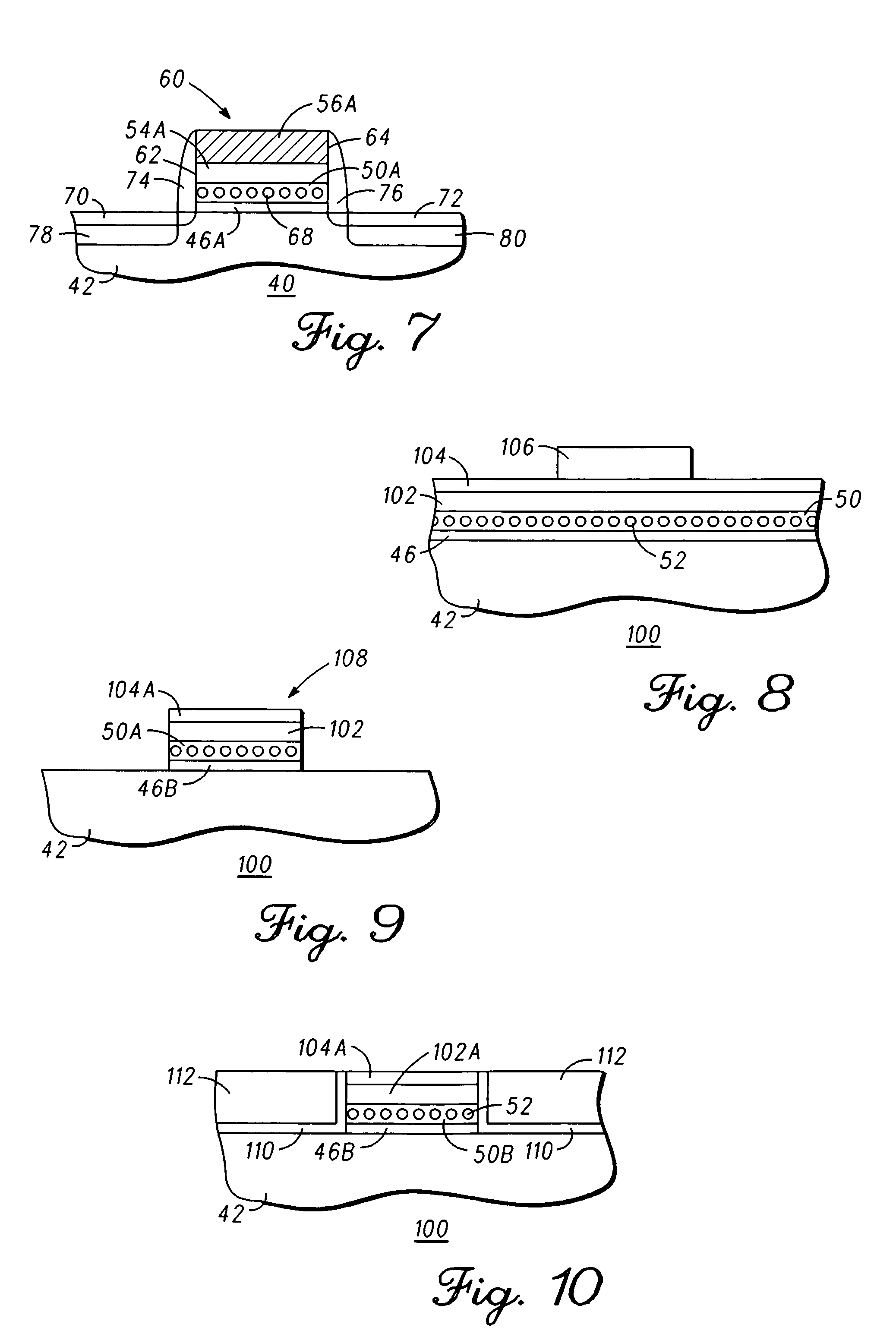
[0024]FIG. 2 is an enlarged cross-sectional side view of a portion of a partially completed memory device 40 during processing in accordance with an embodiment of the present invention. What is shown in FIG. 2 is a semiconductor substrate 42 having a major surface 44. Suitable materials for substrate 42 include silicon, germanium, Semiconductor-On-Insulator (SOI), silicon germanium, gallium arsenide, indium phosphide, other compound semiconductor materials, or the like. The semiconductor material may also be a semiconductor substrate having an epitaxial layer formed thereon. A layer of dielectric material 46 having a thickness ranging from about 20 Angstroms (Å) to about 50 Å is formed on substrate 42. By way of example, layer of dielectric material 46 is oxide grown by dry oxidation. It should be noted that the type of dielectric material for dielectric layer 46 and the technique for forming dielectric layer 46 are not limitations of the present invention. A layer of dielectric mat...


PUM

PropertyMeasurementUnit
temperatureaaaaaaaaaa
thicknessaaaaaaaaaa
temperatureaaaaaaaaaa

Abstract

A memory device having a metal nanocrystal charge storage structure and a method for its manufacture. The memory device may be manufactured by forming a first oxide layer on the semiconductor substrate, then disposing a porous dielectric layer on the oxide layer and disposing a second oxide layer on the porous dielectric layer. A layer of electrically conductive material is formed on the second layer of dielectric material. An etch mask is formed on the electrically conductive material. The electrically conductive material and the underlying dielectric layers are anisotropically etched to form a dielectric structure on which a gate electrode is disposed. A metal layer is formed on the dielectric structure and the gate electrode and treated so that portions of the metal layer diffuse into the porous dielectric layer. Then the metal layer is removed.

Description

FIELD OF THE INVENTION[0001]This invention relates, in general, to memory devices and, more particularly, to memory devices having metal nanocrystals in a charge storage region.BACKGROUND OF THE INVENTION[0002]Memory devices are used in a variety of electronic systems including computers, cellular phones, pagers, personal digital assistants, avionic systems, automotive systems, industrial control systems, appliances, etc. Depending on the particular system configuration, the memory devices may be either non-volatile or volatile. A non-volatile memory device retains the data or instructions when the device is turned off or power is removed. A volatile memory device, on the other hand, does not retain the stored data or instructions when the device is turned off. Flash memory has become an important type of non-volatile memory because it is less expensive to manufacture and denser than most other types of memory devices. In addition, Flash memory is electrically erasable and has a lif...

Claims


Application Information

Patent Timeline
Patent Type & Authority Patents(United States)
IPC IPC(8): H01L21/44
CPCB82Y10/00H01L29/7833H01L29/42332H01L21/28273H01L29/40114
Inventor WANG, CONNIE PIN-CHINYOU, LUKRIVOKAPIC, ZORANBESSER, PAUL RAYMONDPANGRLE, SUZETTE KEEFE
Owner ADVANCED MICRO DEVICES INC
Why Eureka
Try Eureka