Method of fabricating nitrogen-containing gate dielectric layer and semiconductor device

a technology of nitrogen-containing gate dielectric layer and semiconductor device, which is applied in the manufacture of semiconductor/solid-state devices, basic electric elements, electric apparatus, etc., can solve the problems of high cost of plasma nitridation process, high cost, and damage to the internal structure of gate dielectric, so as to reduce the leakage current

Active Publication Date: 2007-12-25
UNITED MICROELECTRONICS CORP
View PDF6 Cites 18 Cited by
  • Summary
  • Abstract
  • Description
  • Claims
  • Application Information

AI Technical Summary

Benefits of technology

[0007]Accordingly, at least one objective of the present invention is to provide a method of fabricating a high-quality nitrogen-containing gate dielectric layer capable of reducing leakage current.
[0008]At least a second objective of the present invention is to provide a method of fabricating a semiconductor device capable of processing a plurality of wafers simultaneously inside the same reaction chamber to increase the yield.
[0013]Using the fabricating method of the present invention, a high-quality nitrogen-containing gate dielectric layer is produced so that current leakage and other electrical problems are improved. Furthermore, the present invention permits a plurality of wafers to be simultaneously treated within the same reaction chamber, thereby significantly increasing the yield. Moreover, the method of the present invention can fabricate semiconductor devices with good electrical properties and reliability.

Problems solved by technology

However, this method frequently damages the internal structure of the gate dielectric and leads to quality problems.
Moreover, the cost for carrying out a plasma nitridation process is high.
Thus, it can easily lead to a flatband voltage variation and an increase in the trapped charges inside the gate dielectric layer, a major cause of electrical problems.
In addition, it may affect the threshold voltage, the difference in work function between the substrate and the gate and the reliability of the device and so lead to negative bias and negative bias temperature instability (NBTI) problem resulting in a drop in the performance of the semiconductor device.
Furthermore, the convention method permits a reaction chamber to process only a single wafer at a time, which may result in a bottleneck in production.

Method used


Image

  • Method of fabricating nitrogen-containing gate dielectric layer and semiconductor device
  • Method of fabricating nitrogen-containing gate dielectric layer and semiconductor device
  • Method of fabricating nitrogen-containing gate dielectric layer and semiconductor device

Examples


Embodiment Construction

[0019]Reference will now be made in detail to the present preferred embodiments of the invention, examples of which are illustrated in the accompanying drawings. Wherever possible, the same reference numbers are used in the drawings and the description to refer to the same or like parts.

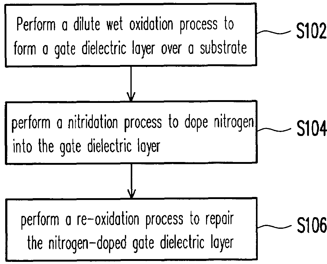
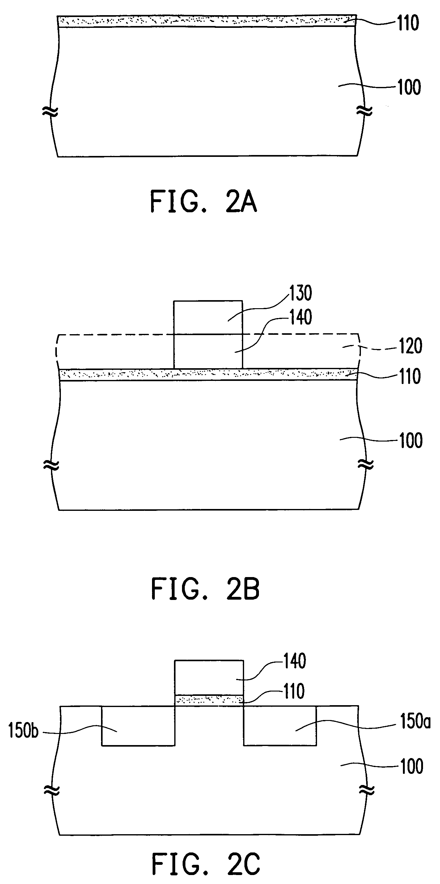
[0020]FIG. 1 is a block diagram showing the steps for fabricating a gate dielectric layer according to one preferred embodiment of the present invention. FIGS. 2A through 2C are schematic cross-sectional views showing the steps for fabricating a metal-oxide-semiconductor according to one preferred embodiment of the present invention. As shown in FIG. 2A, an n-type semiconductor substrate 100 is provided. Thereafter, a nitrogen-containing gate dielectric layer 110 is formed over the semiconductor substrate 100. The method of forming the nitrogen-containing gate dielectric layer 110 includes the following steps.

[0021]First, as shown in FIG. 1, a dilute wet oxidation process is carried out to form the g...


PUM


Abstract

A method of fabricating a nitrogen-containing gate dielectric layer is described. First, a gate dielectric layer is formed on a substrate by performing a dilute wet oxidation process. Then, a nitridation step is performed for doping nitrogen into the gate dielectric layer. After that, a re-oxidation step is performed for repairing the nitrogen-doped gate dielectric layer. The above steps are carried out inside the same reaction chamber. Moreover, two or more wafers can be treated inside the reaction chamber at the same time.

Description

BACKGROUND OF THE INVENTION[0001]1. Field of the Invention[0002]The present invention relates to a method of fabricating semiconductor. More particularly, the present invention relates to a method of fabricating a nitrogen-containing gate dielectric layer and a semiconductor device.[0003]2. Description of the Related Art[0004]With the progressive drop in the dimension of the metal-oxide-semiconductor (MOS) transistor s, more stringent quality requirements are set up for the gate dielectric layer. When the dimension of a MOS transistor drops to a value smaller than 0.1 μm, the thickness of a gate dielectric layer fabricated using silicon oxide layer must also be reduced to a value below 20 Å. As the thickness of the gate dielectric layer grows thinner and thinner, electrons can easily tunnel through the layer to produce a leakage current if there is any defect in the gate dielectric layer.[0005]Therefore, if the gate dielectric layer is fabricated using silicon oxide material, then a...

Claims


Application Information

Patent Timeline
Patent Type & Authority Patents(United States)
IPC IPC(8): H01L21/4763H01L21/3205
CPCH01L21/28202H01L21/3144H01L21/31675H01L21/02238H01L21/0214H01L21/02332
Inventor WANG, YU-RENYEN, YING-WEICHAN, MICHAEL
Owner UNITED MICROELECTRONICS CORP
Why Eureka
Try Eureka