Printed circuit board with embedded capacitors and manufacturing method thereof

a technology of embedded capacitors and printed circuit boards, which is applied in the direction of printed element electric connection formation, electrical apparatus construction details, and metal adhesion improvement. it can solve the problems of inactive fabrication of embedded capacitors, end portions of copper foils, and inability to meet the requirements of high reliability, high capacitance, and simple preparation process

Inactive Publication Date: 2008-02-05
SAMSUNG ELECTRO MECHANICS CO LTD
View PDF16 Cites 29 Cited by
  • Summary
  • Abstract
  • Description
  • Claims
  • Application Information

AI Technical Summary

Benefits of technology

[0073]Therefore, a sludge which is in a mixed composite form of BaTiO3 ceramic powders having high-dielectric constant and a thermosetting plastic epoxy resin or polyimide is printed on the ground layer copper foil formed on the inner layer of the multi-layered printed circuit board, and is semi-dried to a state of the B-stage, and the power layer copper foil is coated on the sludge layer. Thereby, the printed circuit board having embedded decoupling capacitors can be manufactured, which is advantageous in terms of high capacitance, simple preparation process and high reliability.

Problems solved by technology

However, the embedded capacitor PCB has not yet been actively fabricated.
Therefore, standard technology for fabrication of the embedded capacitor PCB has not been established up to now, and a commercially available process technology is still under study.
However, the above printed capacitors have a thickness of 10 μm, and thus end portions of the copper foils 43a and 43b for negative electrodes become cracked.
In addition, the above manufacturing process is disadvantageous in terms of the non-uniform insulation distance between a first layer and a second layer shown in FIG. 1e.
Such a difference in the insulation distance between the first layer and the second layer results in poor impedance of signal circuit in the first and the second layers.
Further, the above process has the drawback, such as generation of a foreign substance by printing and drying of the capacitor pastes 45a and 45b and the copper pastes 46a and 46b.
However, the above manufacturing process according to the second embodiment of conventional techniques is disadvantageous in terms of its high manufacturing cost.
Thus, cost required for fabrication of such capacitors increases.
Hence, when small numbers of the embedded capacitors are realized, large amounts of photo-dielectric positive resin are used, thus increasing loss of materials.
Further, the above process suffers from generation of short between the bottom electrodes 24.
However, in the above manufacturing process according to the third embodiment of conventional techniques, there is the problem of low capacitance, due to low dielectric constant of the embedded capacitor layer.
Thus limitations are imposed on fabrication of the embedded capacitor.
Further, in the above process, there is another problem, such as a thickened PCB due to insertion of the embedded capacitor.
That is, with the intention of obtaining high capacitance by means of the FR-4 dielectric, large numbers of embedded capacitor layers should be inserted, whereby the number of the layers of the PCB increases and the PCB becomes thick, thus increasing a manufacturing cost.
In addition, a further problem in the above manufacturing process is that, upon patterning the upper copper foil for use as a power electrode and the lower copper foil for use as a ground electrode, the thin dielectric film used to obtain high capacitance is subjected to the PCB fabrication process including lamination and patterning of the dry film, thereby causing shorts and cracks between the power electrode and the ground electrode, as shown in FIG. 5.
Specifically, FIG. 5 shows the problem of the PCB embedded with the capacitor formed by insertion of the dielectric having capacitance properties.

Method used


Image

  • Printed circuit board with embedded capacitors and manufacturing method thereof
  • Printed circuit board with embedded capacitors and manufacturing method thereof
  • Printed circuit board with embedded capacitors and manufacturing method thereof

Examples


Embodiment Construction

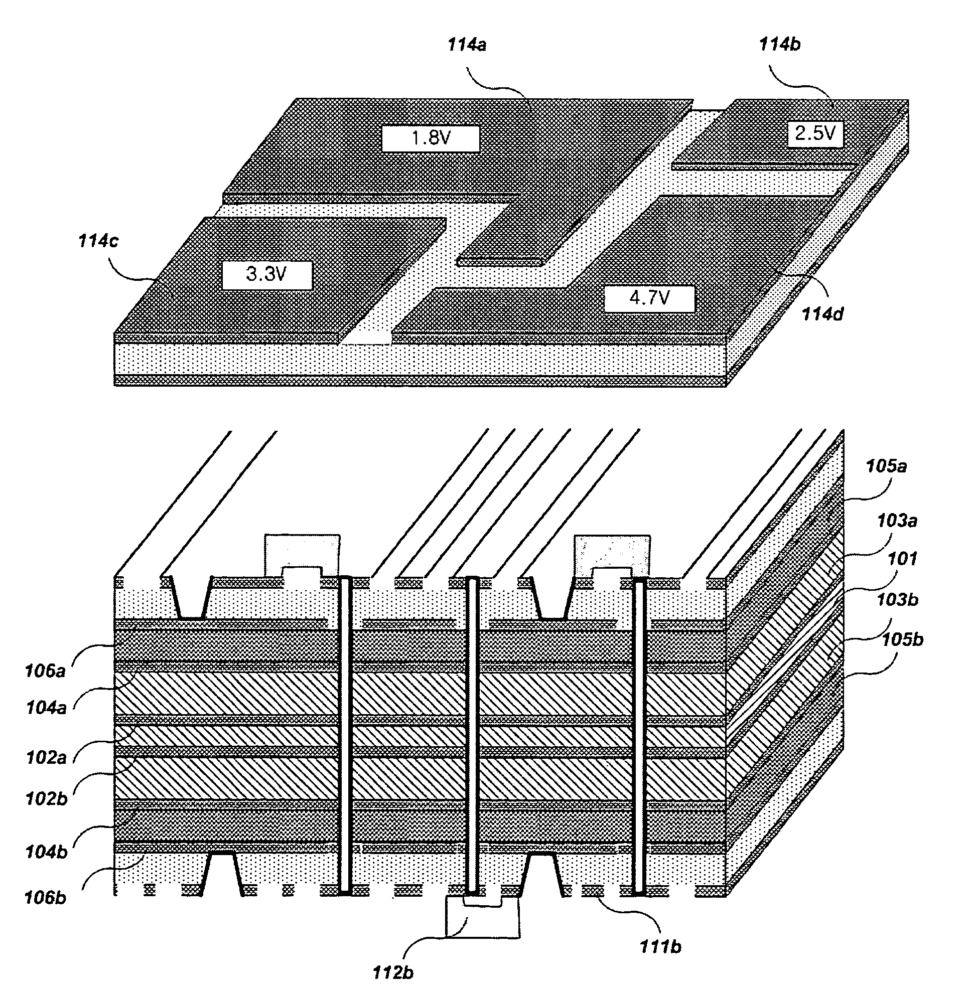
[0082]Below, a detailed description will be given of a printed circuit board with embedded capacitor according to the present invention and a manufacturing method thereof, with reference to the accompanying drawings.

[0083]FIG. 6 is a cross-sectional view of a printed circuit board having embedded capacitors, which is high in capacitance, by coating a capacitor paste having high-dielectric constant on the printed circuit board.

[0084]Referring to FIG. 6, high-dielectric constant of polymer capacitor pastes 105a and 105b are coated on both sides of an inner layer of a printed circuit board (PCB), and are semi-dried to a state of B-stage, thereby fabricating the PCB with embedded capacitors having high capacitance.

[0085]In this regard, BaTiO3 ceramic powders having high-dielectric constant are mixed with a thermosetting plastic epoxy or polyimide to make a sludge in the composite form, any one side of which is printed on the ground layer copper foil or the power layer copper foil in the...


PUM


Abstract

Disclosed is a printed circuit board which is advantageous in terms of high capacitance by embedding capacitors comprising polymer capacitor pastes with high-dielectric constant coated on an inner layer of the printed circuit board and then semi-dried to a state of B-stage.

Description

BACKGROUND OF THE INVENTION[0001]1. Field of the Invention[0002]The present invention relates to printed circuit boards with embedded capacitors, and manufacturing methods thereof. More specifically, the present invention is directed to a printed circuit board having embedded capacitors which is advantageous in terms of high capacitance, resulting from coating high-dielectric constant of a polymer capacitor paste on an inner layer of the printed circuit board and semi-drying the coated capacitor paste to a state of B-stage, and a method of manufacturing the same.[0003]2. Description of the Prior Art[0004]Although discrete chip resistors or discrete chip capacitors have been generally mounted on a printed circuit board (PCB), in recent years, PCBs having passive components such as resistors or capacitors embedded therein are under development.[0005]Such embedded passive components technology for PCBs is set to embed passive components such as resistors or capacitors into the PCB by m...

Claims


Application Information

Patent Timeline
Patent Type & Authority Patents(United States)
IPC IPC(8): H05K1/16H05K3/46H05K3/38H05K3/42
CPCH05K1/162H05K3/382H05K3/429H05K3/4652H05K2201/0209H05K2201/0355H05K2201/093H05K2201/09309H05K2201/09509H05K2201/09663H05K2201/09718H05K3/46
Inventor LEE, SEOK-KYUMIN, BYOUNG-YOULJIN, HYUN-JUKANG, JANG-KYU
Owner SAMSUNG ELECTRO MECHANICS CO LTD
Why Eureka
Try Eureka