
Semiconductor laser device and semiconductor optical modulator

a laser device and semiconductor technology, applied in the direction of lasers, bulk negative resistance devices, semiconductor lasers, etc., can solve the problems of increased threshold current and deterioration of device characteristics, and achieve the effects of reducing thickness, enhancing e, and reducing the probability of carriers being able to exist in quantum wells

Active Publication Date: 2008-02-12
LUMENTUM JAPAN INC
View PDF5 Cites 6 Cited by
  • Summary
  • Abstract
  • Description
  • Claims
  • Application Information

AI Technical Summary

Benefits of technology

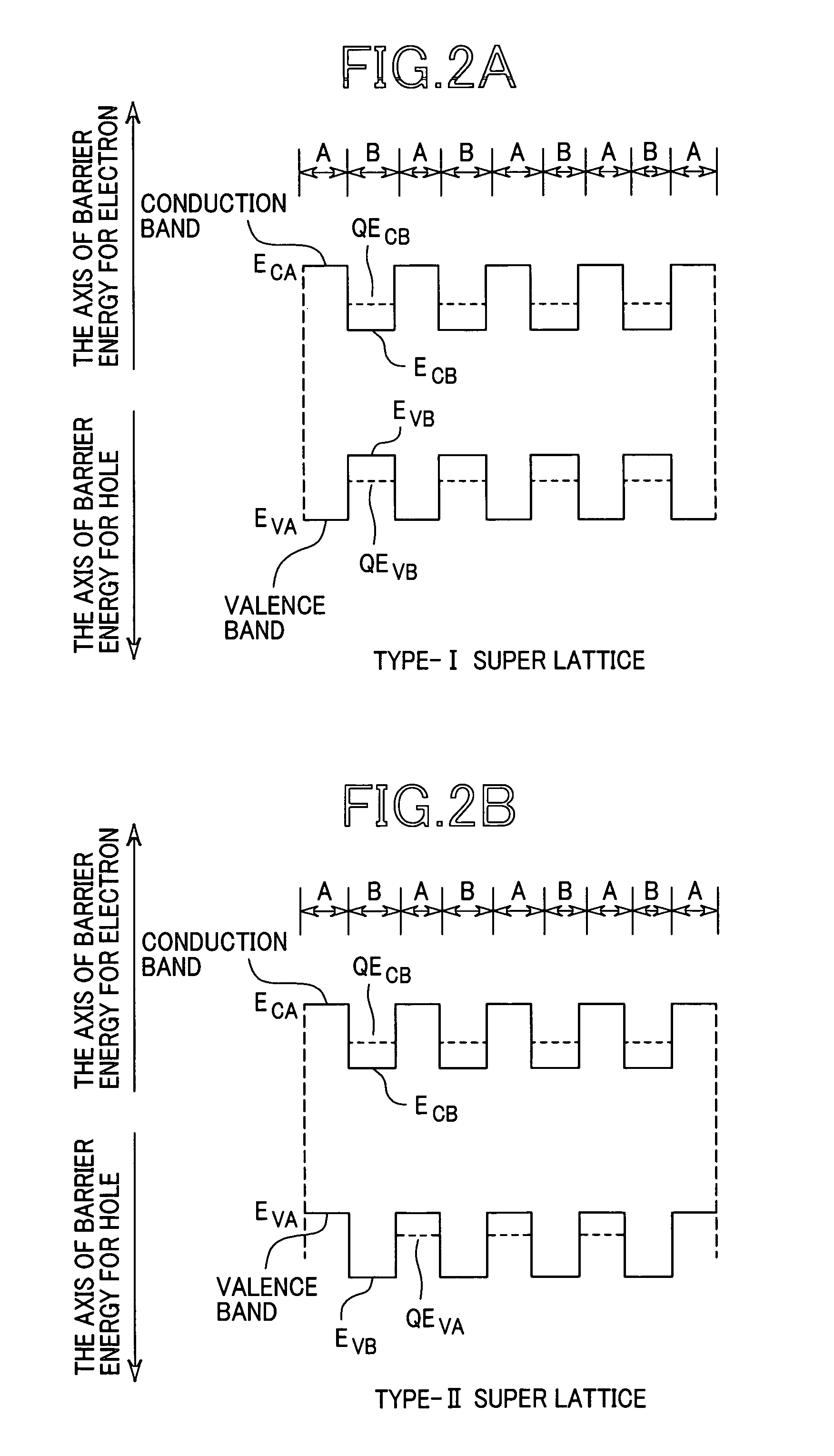
The invention aims to improve the device characteristics of semiconductor devices that include different kind of group-V atom layers. The technical effect of the invention is to reduce the energy band difference at the interface between the layers, which can impede the smooth injection of carriers and affect the device performance. The invention proposes the use of a type-I superlattice layer that allows for the confinement of electrons and holes within a quantum well layer, thus reducing the energy barrier for electrons and holes and improving the device performance.

Problems solved by technology

This heterointerface also impedes the smooth injection of holes and could cause the deterioration of the device characteristics such as an increased threshold current.

Method used


Image

  • Semiconductor laser device and semiconductor optical modulator
  • Semiconductor laser device and semiconductor optical modulator
  • Semiconductor laser device and semiconductor optical modulator

Examples


first embodiment

[0045]Manufacture of a low-resistance AlGaInAs electro-absorption optical modulator according to the present invention will be described in detail below as a first embodiment of the invention. A structural view of the device is shown in FIG. 8. This embodiment assumes that metal-organic chemical vapor deposition (MOCVD) is used as a growth method. In this MOCVD method, triethylgallium (TEG), trimethylindium (TMI), and trimethylaluminum (TMAl) are used as supply sources of group-III elements, and arsine (AsH3) and phosphine (PH3) are used as supply sources of group-V elements. Also, disilane (Si2H6) is used as an n-type doping gas, and dimethylzinc (DMZn), as a p-type doping gas. However, since it is possible to obtain similar effects to the present invention if a structure equivalent to the device structure described herein can be formed, the growth method and the kinds of source materials which can be used are not limited only to those described above.

[0046]An n-type InP substrate ...

second embodiment

[0049]Manufacture of a GaInNAs semiconductor laser according to the present invention will be described in detail below as a second embodiment of the invention. A structural view of the device is shown in FIG. 10. To use GaInNAs as an active layer, it is advantageous to adopt a non-equilibrium growth method during introduction of N, and in addition to the MOCVD method, a molecular beam epitaxial (MBE) method or the like is suitable as such a growth method. This embodiment assumes that gas-source MBE (GS-MBE) is used as the growth method. In the GS-MBE method, gallium (Ga) and indium (In) are used as supply sources of group-III elements, and as supply sources of group-V elements, AsH3 is used for arsenic (As) and PH3 is used for phosphorus (P). Also, silicon (Si) and beryllium (Be) are used as an n-type and a p-type doping material, respectively. If an similar doping concentration is achievable, zinc (Zn) or carbon (C) may be used as an alternative to the above p-type doping material...


PUM


Abstract

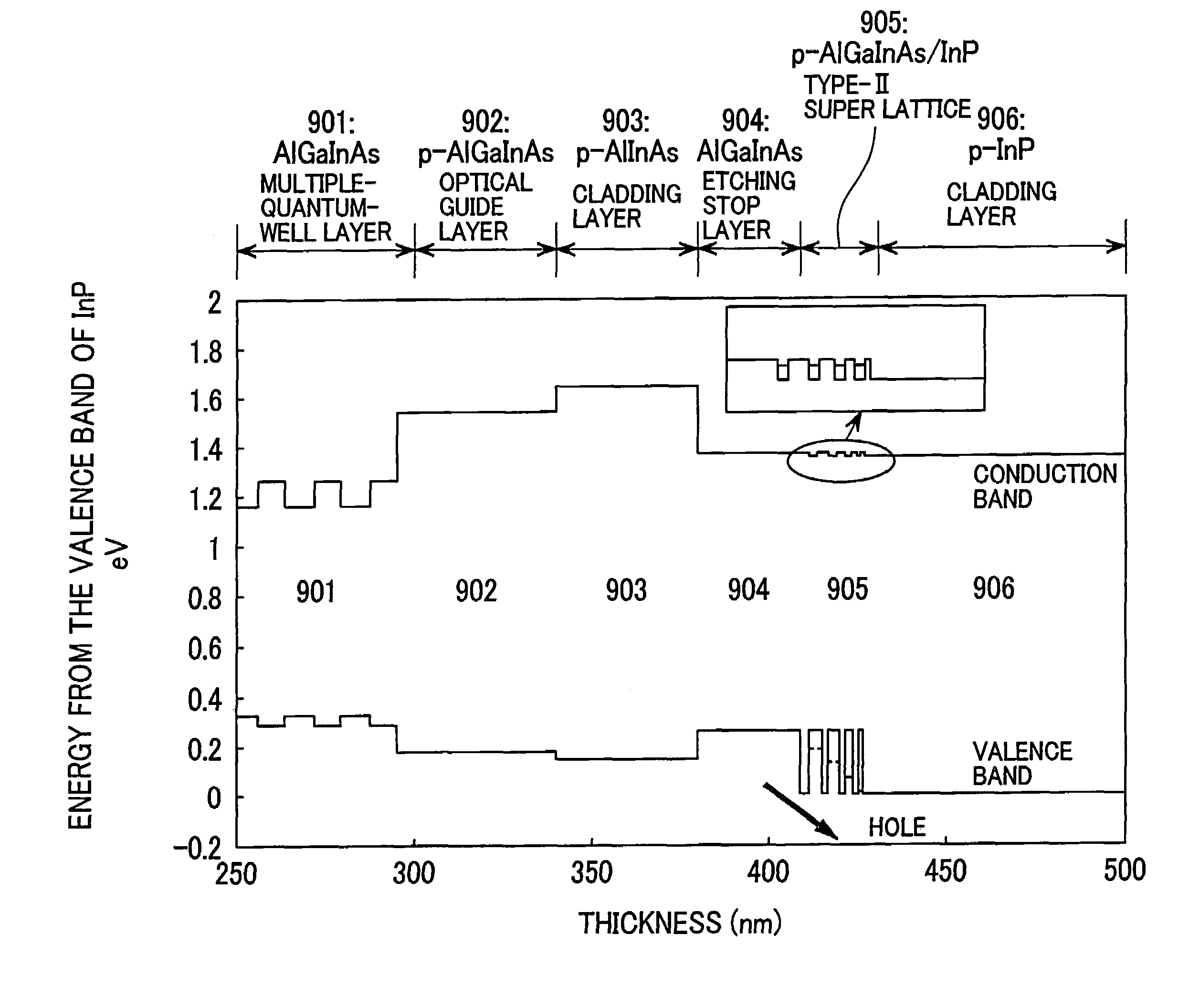
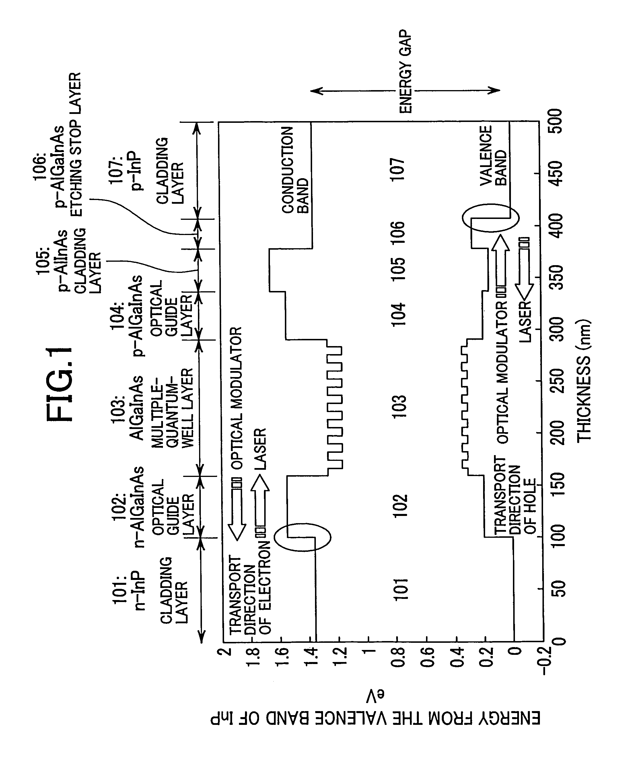
Since the semiconductor devices including a stacked structure of group-III-V alloy semiconductor layers different in the kind of group-V constituent atom form the so-called band line-up of type II, band discontinuity in the heterostructure has impeded smooth transport of carriers and deteriorated device characteristics.According to the present invention, an energy band structure that makes it possible, in one energy band (e.g., a valence band), to smoothly transport carriers of one of two kinds (e.g., holes) by connecting energy discontinuity in an inclined form or stepwise, and at the same, in the other energy band (e.g., a conduction band), to maintain a barrier effect for carriers of the other kind (e.g., electrons) by retaining energy discontinuity, can be realized for improved transport characteristics of carriers at the heterointerface forming the band line-up of type II.

Description

CLAIM OF PRIORITY[0001]The present application claims priority from Japanese application JP 2005-122016, filed on Apr. 20, 2005, the content of which is hereby incorporated by reference into this application.BACKGROUND OF THE INVENTION[0002]1. Field of the Invention[0003]The present invention relates to semiconductor optical devices, and more particularly, to a technology for improving the transport characteristics of carriers at heterointerfaces.[0004]2. Description of the Related Art[0005]Recently, the demands for greater transmission capacities are rapidly growing with factors such as the explosive increase in the Internet users. The transmission speeds of Gbps levels, that have traditionally been used for trunk-system optical communications networks, should be necessary after 5-10 years for the networks relatively short in transmission distance such as LAN or MAN. It will be essential that, in addition to the high-speed modulation characteristics mentioned above, the optical mod...

Claims


Application Information

Patent Timeline
Patent Type & Authority Patents(United States)
IPC IPC(8): H01L29/02H01L47/00H10N80/00
CPCB82Y20/00H01S5/34313H01S5/2009H01S5/3213H01S5/3216H01S5/34306H01S5/34366H01S2304/04
Inventor KITATANI, TAKESHIAOKI, MASAHIROTSUCHIYA, TOMONOBU
Owner LUMENTUM JAPAN INC
Learn More