[0020] In the example described in the Journal of Applied
Physics, Vol. 73, 1993, p. 21, at a GaAs / AlAs type-I heterointerface, a type-I
superlattice structure using these materials is introduced to improve the transport characteristics of carriers. The thickness of the GaAs layer in the
superlattice decreases gradually from the GaAs layer side toward the AlAs layer side of the heterointerface, whereas the thickness of the AlAs layer in the
superlattice gradually increases from the GaAs layer side toward the AlAs layer side of the heterointerface. Thus, the energy values of the
quantum levels formed in both the
conduction band and
valence band of the superlattice can be raised gradually from the GaAs layer, side toward the AlAs layer side, as a result both the
conduction band and the
valence band can be connected smoothly. When this concept is applied to a heterostructure of type-II heterointerface, same effects can also be obtained by applying a gradual change in thickness similar to the above. Consequently, as denoted by a dotted line near a heterointerface in FIG. 5A, a band energy difference at the heterointerface can be reduced simultaneously in the conduction band and the valence band. This is the way the band connection according to a conventional technology is implemented.
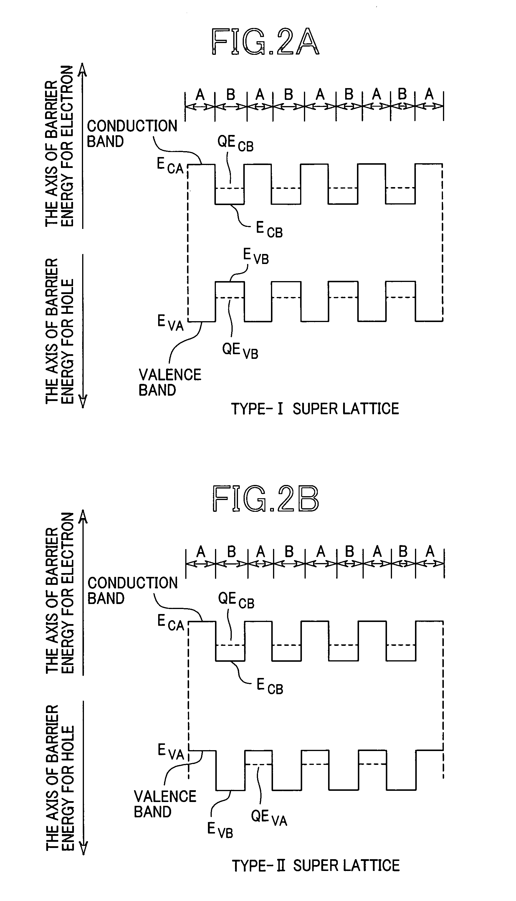
[0022] In the conventional technology of FIG. 5A, since the conduction band and the valence band are connected smoothly at the same time, although the transport probability of one kind of carrier (e.g., holes) improves, the possibility of the other kind of carrier (e.g., electrons) leaking out in the same direction is also enhanced at the same time. To solve this problem, the band structure of FIG. 5B is considered to be desirable. That is, carriers of one of two kinds (e.g., holes) are transported smoothly by reducing the band energy difference in one energy band (e.g., valence band) stepwise, and leakage of carriers of the other kind (e.g., electrons) from heterointerfaces is prevented by connecting the other energy band (e.g., conduction band) so as to maintain the discontinuity of the band energy difference. Conventionally, a specific method of achieving such band structure has not been invented.
[0023] Japanese Patent Laid-open No. 10-27925 is described below as yet another example of a conventional technology. An energy band diagram of a device is shown in FIG. 6. This example relates to a structure in which a type-II superlattice 602 made up of ZnTe and ZnSe is introduced between the p-ZnTe 601 and n-ZnSe 603 which are group-II-VI
alloy semiconductors. Thicknesses of ZnTe layer in the superlattice is set to 0.3 nm, 0.6 nm, 0.9 nm, 1.2 nm, 1.5 nm, 1.8 nm, 2.4 nm, 3.0 nm, and 5.0 nm, and thicknesses of ZnSe layer in the superlattice are set to a fixed value of 5.0 nm. The
quantum level of a valence band gradually increases from the p-ZnTe 601 side toward the n-ZnSe 603 side. Under a forward bias condition, these
quantum levels are lined up and this improves the injection efficiency of holes from the p-ZnTe 601 into the n-ZnSe 603. In a conduction band, however, since the thickness of ZnSe layer in superlattice is 5.0 nm, the electrons in the n-ZnSe 603 leak out into the ZnTe / ZnSe superlattice layer 602. This example, therefore, conceptually differs from the new band structure in FIG. 5B that the present inventors invented.
[0029] The thickness of the layer in the superlattice layer where the energy position of a
quantum level is to be increased stepwise can be obtained by gradually reducing the thickness once it has been increased to 100 nm as a maximum allowable sufficient thickness for obtaining a quantum effect. A minimum allowable thickness value at that time is about 0.2 nm, which is equivalent to one atomic layer of thickness. Next, studies were conducted on the thickness of the layer at which the band energy difference is to be kept discontinuous. The probability of carriers being able to exist in a
quantum well can be reduced by enhancing E to a value close to V, so that the carriers can be prevented from entering the
quantum well. More specifically, E can be enhanced by reducing “d”. Formation of such a
quantum level at an energy position allows the band energy difference at a semiconductor heterointerface to be kept discontinuous.
[0030] It can be seen from the results of FIG. 4 that when “d” is 3.0 nm, E can be raised to an energy value equivalent to about 70% of V. Forming such a
quantum level allows the band energy difference at the semiconductor heterointerface to be effectively kept discontinuous. The
layer thickness for retaining the band energy difference is therefore defined as any desired value
ranging from a minimum allowable value of 0.2 nm equivalent to one atomic layer of thickness, to a maximum allowable value of 3.0 nm. The
barrier effect can be maintained, even if the
layer thickness slightly fluctuates within this
layer thickness range of the superlattice. Although the energy positions of quantum levels more or less change according to the kinds of
semiconductor materials constituting the heterointerface, a sufficient
barrier effect can be obtained even if the thickness of the
quantum well layer is 3.0 nm or less. This layer thickness range is equivalent to the fact that the
barrier layer is sufficiently thin at the opposite band where the energy position of the quantum level is to be increased stepwise, and it is possible, by utilizing a tunneling effect, even to improve a transport probability of carriers significantly. These synergetic effects allow carrier transport characteristics to be significantly improved by introducing the superlattice structure of the present invention.
[0032] According to the present invention, it is possible to enhance a confinement effect of carriers within quantum well active
layers of a semiconductor
laser, thus improving its high-temperature characteristics, and obtaining large gains of the active
layers. Thus, a semiconductor
laser excellent in high-temperature high-speed modulation characteristics can be realized. A improvement of carrier conversion efficiency and of an
extinction characteristics are also expected in an electro-absorption
optical modulator and the like.

