Exposure apparatus, and device manufacturing method using the same

a technology of refraction and apparatus, applied in the field of exposition apparatus, can solve the problems of limiting the use of ultraviolet light in lithography, the limitation of the refraction of light in the visible light region or in the wavelength region of the lens system, and the rapid miniaturization of the semiconductor devi

Inactive Publication Date: 2008-02-12
CANON KK
View PDF34 Cites 10 Cited by
  • Summary
  • Abstract
  • Description
  • Claims
  • Application Information

AI Technical Summary

Benefits of technology

[0034]In one preferred form, the cold trap may include a radiation shield member effective to prevent radiation cooling of a predetermined member by the cold trap. The predetermined member may be at least one of the reflective optical elements.

Problems solved by technology

However, semiconductor devices are being miniaturized rapidly, and there is a limit in the lithography using ultraviolet light as described above.
Therefore, a lens system that is based on refraction of light and that can be used in a visible light region or in a wavelength region of ultraviolet light such as described above, is not practical and a reflection optical system is used in place of it.
However, since the degree of freedom in optical design is small, it is difficult to incorporate a total reflection mirror into a projection optical system.
The reflectance of a multilayered-film mirror with respect to EUV light is about 0.7 at the best, and thus there is a large loss of light quantity at each multilayered-film mirror.
Thus, there is a possibility that, due to this heat, the multilayered-film mirror may expand or deform thereby to cause degradation of the performance of the whole optical system.
Although the utilization efficiency of EUV light is higher with a smaller number of mirrors, aberration correction becomes more difficult to achieve.
To this end, the exposure apparatus is equipped with many driving mechanisms, and this leads to a possibility that, due to friction or the like, outgassing that may cause a decrease of mirror transmittance is produced.
Since outgassing from a member having a large surface area such as above can not easily be removed completely, there is a difficulty in providing high vacuum in the exposure space.
Moreover, while wafers are loaded into the exposure apparatus from the outside atmosphere, during the wafer loading it is very difficult to remove air components, containing moisture, adhered to each wafer in a short time period.
Because of these outgassing from the wafer or the resist, it is very difficult to maintain a high-vacuum condition as described above.
This leads to degradation of the throughput.

Method used


Image

  • Exposure apparatus, and device manufacturing method using the same
  • Exposure apparatus, and device manufacturing method using the same
  • Exposure apparatus, and device manufacturing method using the same

Examples


first embodiment

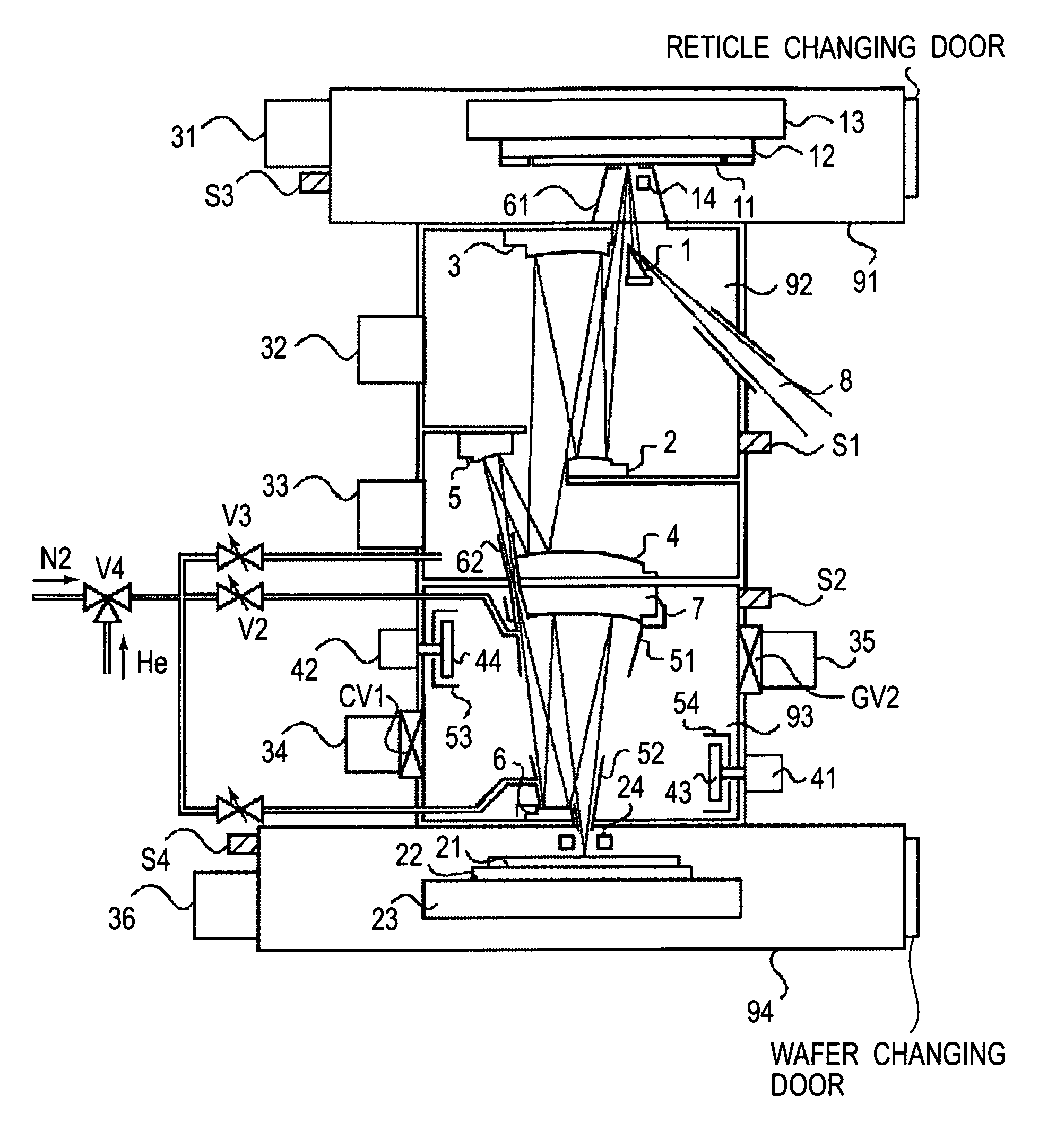
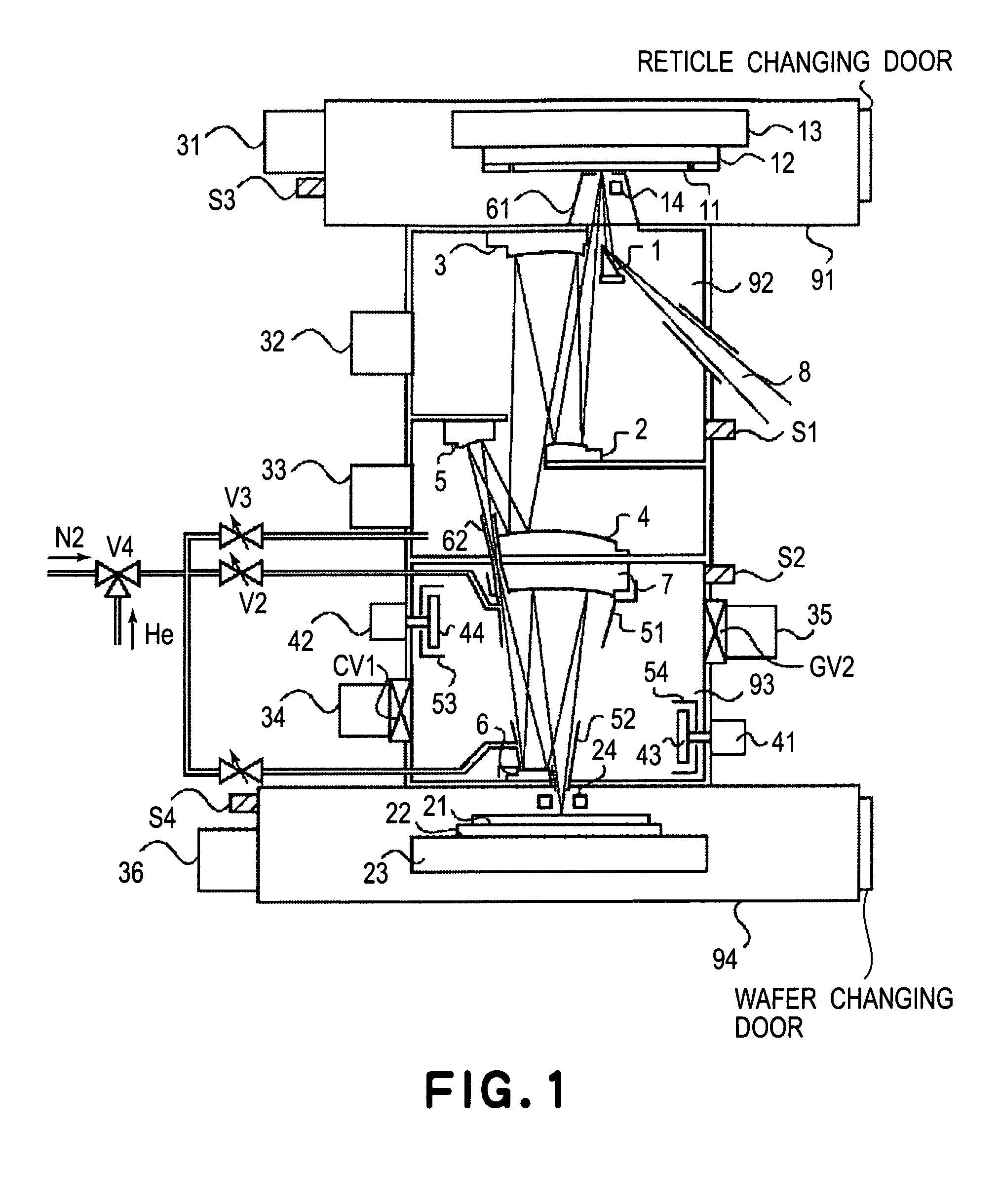
[0061]FIG. 1 is a side view schematically showing the structure of a lithographic system according to one preferred embodiment of the present invention.

[0062]In FIG. 1, denoted at 11 is a reflection type reticle, and denoted at 12 is a reticle holding device for holding the reticle 11. Denoted at 13 is a reticle stage for moving the reticle 11 as held by the reticle holding device. Denoted at 8 is extreme ultraviolet (EUV) light that is exposure light. Denoted at 1 is a reticle illuminating mirror, and denoted at 2-7 are first to sixth mirrors that constitute a projection optical system. Denoted at 14 is a reticle alignment optical system. Denoted at 21 is a wafer, and denoted at 22 is a wafer chuck for holding the wafer 21. Denoted at 23 is a wafer stage for moving the wafer 21 as held by the wafer chuck 22, and denoted at 24 is a wafer alignment optical system.

[0063]The EUV light source comprises a laser plasma light source, not shown. It has such structure that a pulse laser ligh...

second embodiment

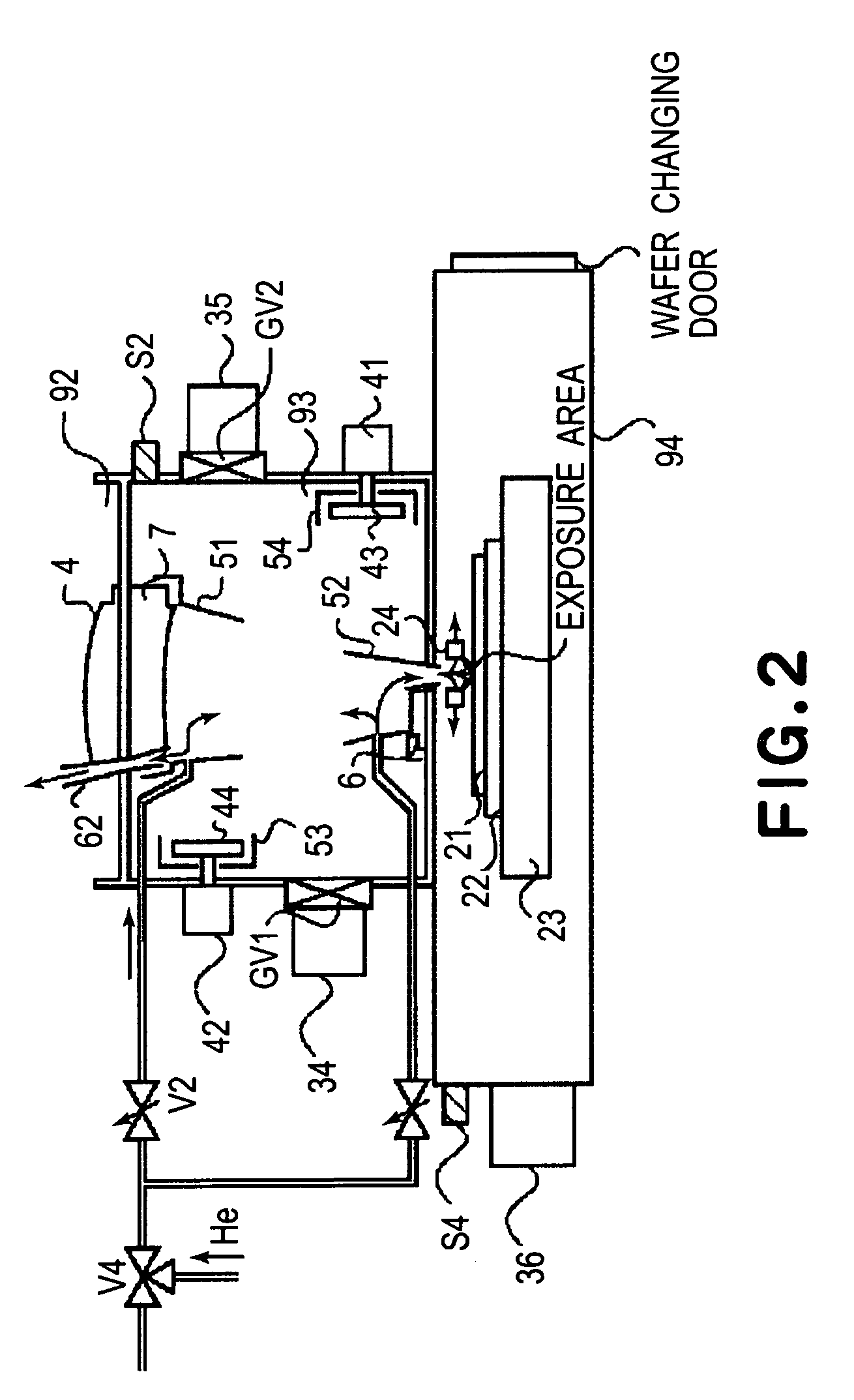
[0099]FIG. 4 illustrates a structure according to a second embodiment of the present invention. FIG. 4 is an enlarged view of a portion around a fifth mirror 6 of the projection system. In this embodiment, a cryo-panel is disposed at a right-hand side of the fifth mirror 6 of the projection system, the cryo-panel having an opening for allowing passage of exposure light and having a radiation shield at its periphery. Like the first embodiment, gasses are supplied during the exposure process and during reactivation of the cryo-panel.

[0100]With the disposition of the cryo-panel 45 above the exposure area on the wafer surface, the path of contamination (contaminant substances) which might otherwise enter the light path space 93 due to scattering is deflected by the helium gas supplied through the valve V1. As a result, the probability that the contamination impinges on the cryo-panel 45 and is attracted (exhausted) thereby increases.

[0101]FIG. 5 illustrates this effect, being analyzed o...

third embodiment

[0113]Next, referring to FIGS. 9 and 10, an embodiment of a device manufacturing method which uses an exposure apparatus described above, will be explained.

[0114]FIG. 9 is a flow chart for explaining the procedure of manufacturing various microdevices such as semiconductor chips (e.g., ICs or LSIs), liquid crystal panels, or CCDs, for example. Step 1 is a design process for designing a circuit of a semiconductor device. Step 2 is a process for making a mask on the basis of the circuit pattern design. Step 3 is a process for preparing a wafer by using a material such as silicon. Step 4 is a wafer process which is called a pre-process wherein, by using the thus prepared mask and wafer, a circuit is formed on the wafer in practice, in accordance with lithography. Step 5 subsequent to this is an assembling step which is called a post-process wherein the wafer having been processed at step 4 is formed into semiconductor chips. This step includes an assembling (dicing and bonding) process...


PUM

PropertyMeasurementUnit
temperatureaaaaaaaaaa
wavelengthaaaaaaaaaa

Abstract

Disclosed is an exposure apparatus having a specific structure that includes a cold trap plate for attracting contaminant substances which might cause a decrease of reflectance of a mirror when adhered thereto, and a radiation shield member for preventing excessive cooling of the mirror or the like by the cold trap plate.

Description

FIELD OF THE INVENTION AND RELATED ART[0001]This invention relates to an exposure apparatus for transferring a fine circuit pattern.[0002]As a lithographic process for production of a fine semiconductor device such as semiconductor memory or logic circuit, there is a reduction projection exposure method using ultraviolet rays.[0003]The smallest size that can be transferred by the reduction projection exposure process is proportional to the wavelength of light used for the transfer, and also it is inversely proportional to the numerical aperture of a projection optical system. This has facilitated shortening of the wavelength of exposure light to be used for transfer of fine circuit patterns, and actually the wavelength of ultraviolet light has been shortened from Hg lamp i-line (wavelength 365 nm) to KrF excimer laser (wavelength 248 nm) and then to ArF excimer laser (wavelength 193 nm).[0004]However, semiconductor devices are being miniaturized rapidly, and there is a limit in the ...

Claims


Application Information

Patent Timeline
Patent Type & Authority Patents(United States)
IPC IPC(8): G03B27/52G03B27/32G03B27/42G03F7/20H01L21/027
CPCG03F7/70891G03F7/70916G03F7/70933
Inventor HASEGAWA, NORIYASU
Owner CANON KK
Why Eureka
Try Eureka