Semiconductor device

a technology of semiconductor devices and semiconductor films, applied in semiconductor devices, semiconductor/solid-state device details, electrical apparatus, etc., can solve the problems of affecting the electrical conductivity of wiring, so as to reduce the resistance value, increase the particle grain diameter of the metallic film, and maintain the effect of surface flatness

Inactive Publication Date: 2008-02-19
RENESAS ELECTRONICS CORP
View PDF8 Cites 16 Cited by
  • Summary
  • Abstract
  • Description
  • Claims
  • Application Information

AI Technical Summary

Benefits of technology

[0054]According to another aspect of the embodiments, the step of diffusing the different metallic element into the upper portion of the metallic film can include heat treating the metallic film. Such heat treating can increase the particle grain diameters of the metallic film, thus reducing a resulting resistance value. Further, the different metallic element can be more uniformly dispersed within the metal of the metallic film at an interface between the main constituent metallic element and the different

Problems solved by technology

However, as miniaturization of device elements has progressed, electromigration (hereinafter referred to as “EM”) has become a problem even for wiring made from copper.
Consequently, EM problems from mass transfer through such grain boundaries can be very pronounced.
Such a phase can result in undesirable differences in the electrical conductivity of the wiring.
Recently, the development of stress migration in copper wirings has become a problem. FIGS. 11(a) and 11(b) are cross sectional views of multi-layer c

Method used


Image

  • Semiconductor device
  • Semiconductor device
  • Semiconductor device

Examples


first embodiment

[0135]A first embodiment can include applying the present invention to a copper wiring according to a dual Damascene method, and will be described with reference to FIG. 2(a) to 3(d).

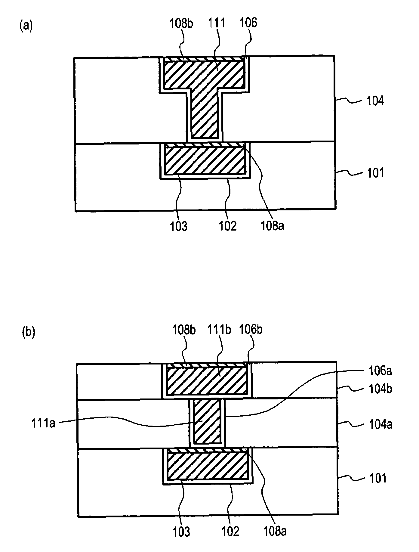
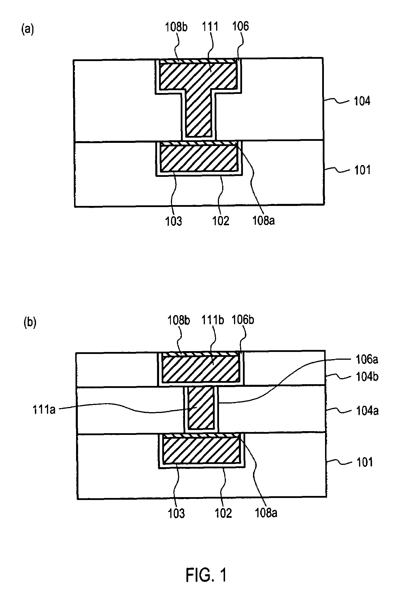
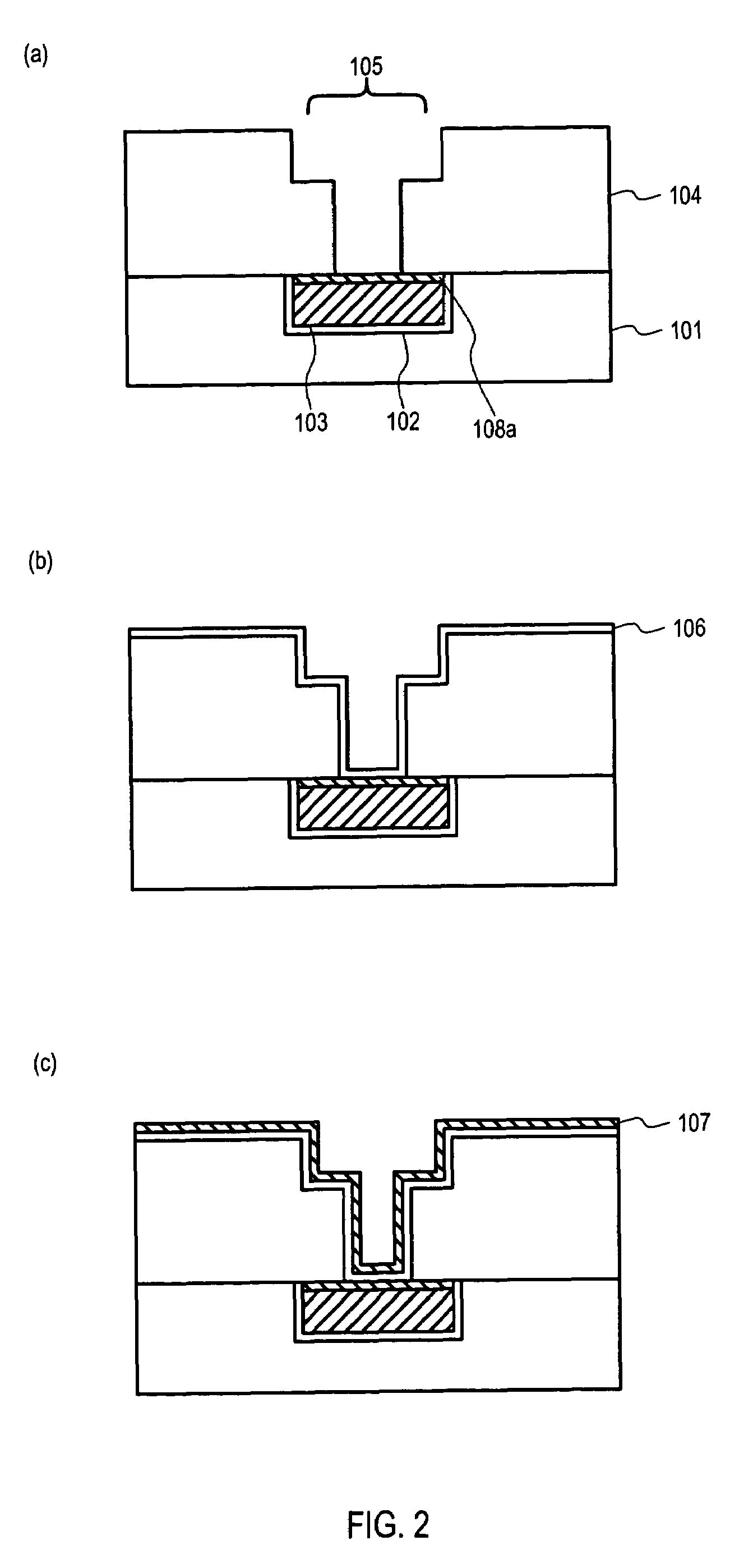
[0136]First, an insulating film 101 can be formed on a silicon substrate (not shown in the figures). A lower layer wiring made from a barrier metal film 102, a copper containing metallic film 103, and silver containing metallic protective film 108a can be formed within insulating film 101. It is noted that formation of a lower layer wiring can be accomplished by processes similar to the procedures described below.

[0137]After forming an interlayer insulating film 104 on insulating film 101, a connection hole can be formed in parts by multi-stage dry etching. This can form a wiring groove 105 having a T shape when viewed in cross section. A state of a semiconductor following the step is shown in FIG. 2(a).

[0138]Subsequently, a barrier metal film 106 can be formed on an entire substrate surface (FIG. 2(b))...

second embodiment

[0158]Further, in the present second embodiment, a copper containing metallic film can be separated into two portions, the connection plug portion 111a and the wiring portion 111b by the barrier metal film 106b disposed between the two. This can suppress deformation of an entire wiring, and developments of a void (like that shown as 122a in FIG. 11(a) as a particular example), can be reduced.

[0159]A third embodiment will now be described. A third embodiment can differ from the above first embodiment in that silver containing metallic protective films 108a and 108b can be formed with a plating solution containing copper and silver. A method of manufacturing a semiconductor device according to this embodiment will be described with reference to FIGS. 2(a) to 2(c) and 4(a) to 4(d).

[0160]First, a seed metallic film 107 can be formed on a barrier metal film 106 by implementing processes from FIGS. 2(a) to 2(c) of the first embodiment. Subsequently, a copper plating film 110 can be formed...


PUM


Abstract

A semiconductor device with a metallic region can have a resistance to stress migration and increased reliability. A lower layer wiring made from a barrier metal film (102) and a copper containing metallic film (103) can be formed within an insulating film (101). An interlayer insulating film (104 or 104a and 104b) can be formed thereon. An upper layer wiring made from a barrier metal film (106 or 106a and 106b) and a copper containing metallic film (111 or 111a and 111b) is formed within the interlayer insulating film (104 or 104a and 104b). A silver containing metallic protective film (108a and 108b) can be formed on surfaces of the lower layer wiring and upper layer wiring.

Description

TECHNICAL FIELD[0001]The present invention relates generally to a semiconductor device, and more particularly to a semiconductor device having a metallic region, and a method of manufacturing the same.BACKGROUND OF THE INVENTION[0002]With the recent demand for very highly integrated circuit devices, copper has become more widely used as a wiring and / or plug material. Copper has the advantageous characteristics of lower resistance and superior electromigration resistance, as compared to aluminum, which has enjoyed wide use up to now.[0003]However, as miniaturization of device elements has progressed, electromigration (hereinafter referred to as “EM”) has become a problem even for wiring made from copper. A copper wiring is typically formed from a copper film formed by a plating method, or the like. In such a case, a resulting copper film has a polycrystalline-structure of aggregate copper grains. If a voltage is applied across a copper wiring having this type of structure, a mass tra...

Claims


Application Information

Patent Timeline
IPC IPC(8): H01L23/48H01L21/3205H01L21/288H01L21/768H01L23/52H01L23/532
CPCH01L21/288H01L21/2885H01L21/76829H01L21/76843H01L21/76849H01L21/76864H01L21/76867H01L21/76877H01L23/53238H01L2924/0002H01L2924/00
Inventor UENO, KAZUYOSHI
Owner RENESAS ELECTRONICS CORP
Why Eureka
Try Eureka