Dual-band active filter

a filter and active technology, applied in the field of microwave circuits, can solve the problems of limited single-band operation, no signal gain, and difficulty in achieving true single-chip implementation, and achieve the effect of enhancing the interference rejection level

Active Publication Date: 2008-03-04
MICROCHIP TECH INC +1
View PDF3 Cites 3 Cited by
  • Summary
  • Abstract
  • Description
  • Claims
  • Application Information

AI Technical Summary

Benefits of technology

[0008]It is another objective of the present invention to provide a dual-band active filter fabricated on the silicon substrate for use in the microwave to millimeter-wave range without degrading the circuit gain and without increasing the chip size.
[0015]The advantage of the dual-band active filter of the present invention is that the match units have filtering performances and the filter responses can be precisely predicted.
[0016]Another advantage of the dual-band active filter of the present invention is the transmission zeros can be designed at the desired frequencies to enhance the interference rejection level.

Problems solved by technology

But the off-chip passive filters, conventionally implemented by waveguide or planar structures on ceramic substrates, are bulky or inherently lossy that they are difficult in achieving true single-chip implementation.
A variety of conventional active filter design methods offer good solution of this difficulty, but they are limited to single-band operation.
They provide no signal gain and, in reality, they have loss due to the substrate and conductor losses.
Although this dual-band LNA provides dual-band gain, it suffers poor stop-band suppression.

Method used


Image

  • Dual-band active filter
  • Dual-band active filter
  • Dual-band active filter

Examples


first embodiment

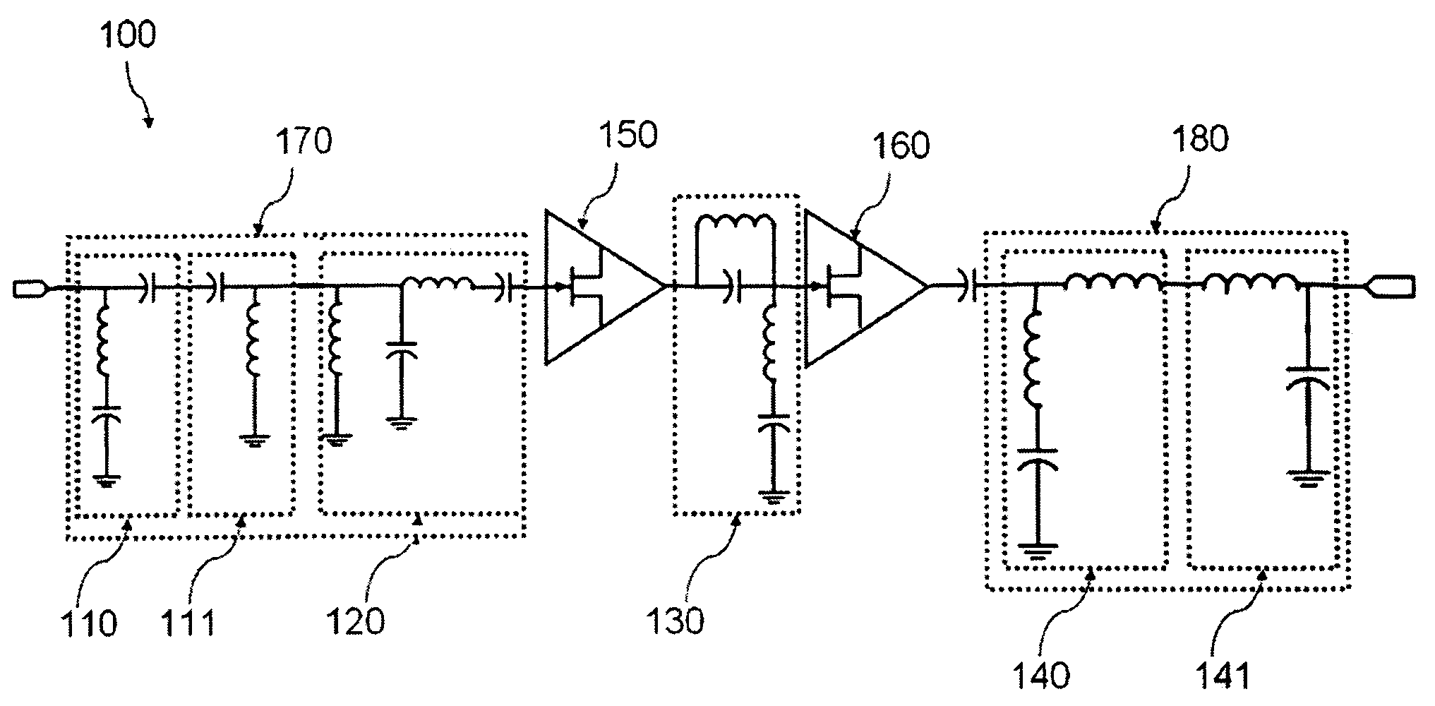
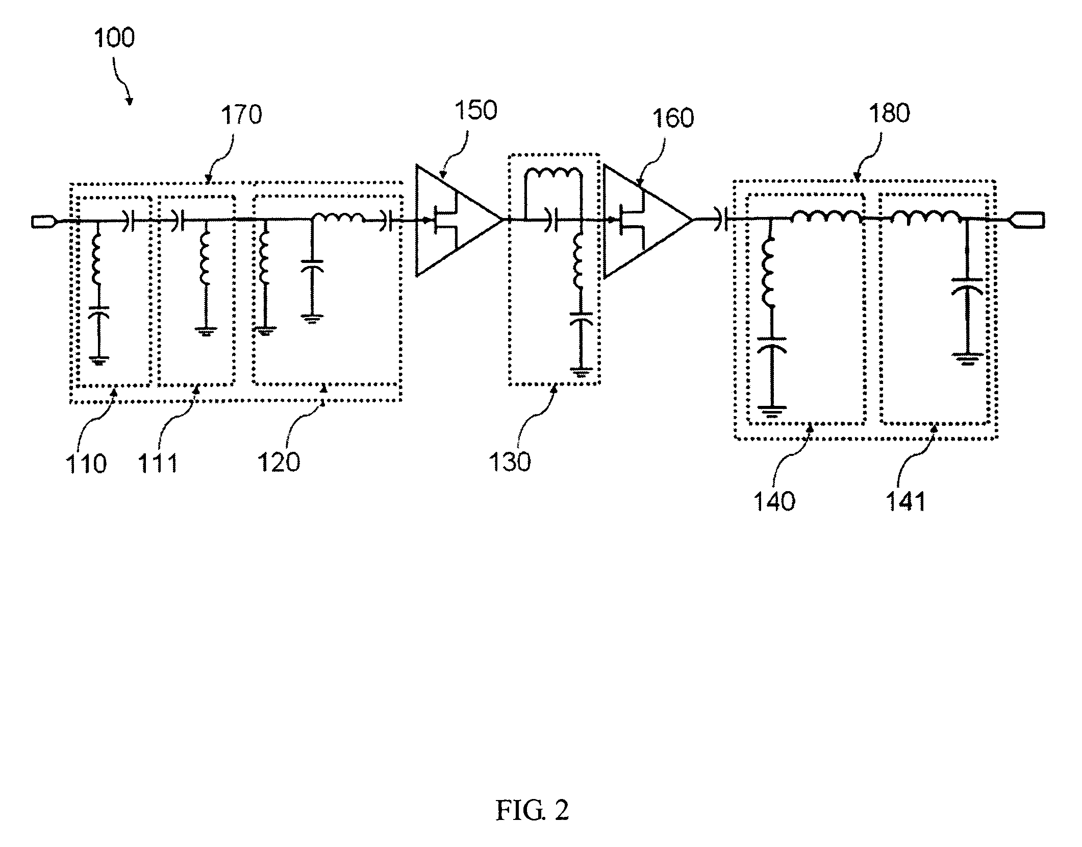
[0034]Now referring to FIG. 2, it shows a schematic of a dual-band active filter according to the present invention. The dual-band active filter 100 comprises an input match unit 170, a first gain stage 150 electrically connected to the first input match unit 170, a first inter-stage unit 130 electrically connected to the first gain stage 150, a second gain stage 160 electrically connected to the first inter stage unit 130 and an output unit 180 electrically connected to the second gain stage 160. As shown in the FIG. 2, the input port of the dual-band active filter is in front of the input match unit 170 and the output port of the dual-band active filter follows the output match unit 180.

[0035]The input match unit 170 is used for gain match of the dual-band active filter 100 and for having a first filter characteristic, preferably a band-pass filter response. The first gain stage 150 is used for providing the flat gain of the dual-band active filter 100. The first inter-stage unit ...

second embodiment

[0059]Now referring to FIG. 9, FIG. 10 and FIG. 11, they show the simulated and measured power gain (insertion loss), input return loss and output return loss performance of the dual-band active filter according to the present invention, respectively. The simulated results show good dual-bandpass performance that the first pass-band gain is 26.6±1.2 dB and return loss is 7.8±0.4 dB from 2.4 to 2.483 GHz and the second pass-band gain is 26.1±0.2 dB and the return loss is 12.4±0.1 dB from 5.1 to 5.35 GHz. The simulated results show that the lower-side stop-band attenuation is 50-dBc below 500 MHz, 52-dBc attenuation level is obtained at 3.9 GHz between the two passband, and higher-side stop-band attenuation is 31-dBc above 8.5 GHz. The measured results show good dual-bandpass performance that the first passband gain is 25.5±0.4 dB and return loss is 8.2±0.2 dB from 2.4 to 2.483 GHz and the second passband gain is 27.1±0.5 dB and the return loss is 11.2±0.3 dB from 5.1 to 5.35 GHz. The...


PUM


Abstract

The present invention discloses a dual-band active filter having filtering response and positive pass-band gain. The dual-band active filter includes an input match unit for gain match of the dual-band active filter and for having a band-pass filtering response; a first gain stage electrically connected to the first input match unit for providing the flat gain of the dual-band active filter; an inter-stage unit electrically connected to the first gain stage for matching gain and for having a band-stop filter response; a second gain stage electrically connected to the inter stage unit for providing the flat gain of the dual-band active filter; and an output unit electrically connected to the second gain stage for matching the dual-band active filter and for having a low-pass filtering response. The dual-band active filter according to the present invention uses the cascade connection of multiple filter stages to have band-pass filtering response at two different frequency bands and obtain high stop-band attenuation by providing plural transmission zeros in the stop-band.

Description

BACKGROUND OF THE INVENTION [0001]1. Field of the Invention[0002]The present invention generally relates to a microwave circuit, and more particularly to a dual-band active filter having positive gain and bandpass spectral performance for microwave and millimeter-wave wireless communication systems.[0003]2. Description of the Related Art[0004]The rapid development of the coexisted operation of multi-standard wireless and mobile communication has been driving conventional RF and baseband transceivers to have integrated multi-band and multi-functional characteristics, such as the multimode wireless LAN IEEE802.11a / b / g PCMCIA card, the integrated Bluetooth / WLAN card, and the integrated GSM / WLAN handset. This requirement has driven the conventional single-band RF circuits, such as the low-noise amplifier (LNA), bandpass filters (BPF), mixers, voltage-controlled oscillators (VCOs) and the power amplifier (PA), to a new design era. Moreover, the fast developing radio-on-a-chip circuit con...

Claims


Application Information

Patent Timeline
Patent Type & Authority Patents(United States)
IPC IPC(8): H04B1/26
CPCH03F1/565H03F3/191H03F3/195H03H11/28H03F2200/111H03F2200/165H03F2200/168H03F2200/171H03F2200/222H03F2200/387H03F2200/411H03F2200/451
Inventor SHENG-FUH, CHANGWEN-LIN, CHENYU-DA, SHIUHUNG-CHENG, CHENSHU-FEN, TANGALBERT, CHEN
Owner MICROCHIP TECH INC
Why Eureka
Try Eureka