Multiple layer etch stop and etching method

a technology of reactive ions and etching stops, which is applied in the field of deep reactive ion etching processes, can solve the problems of difficult to completely remove hard etching stop materials from the back side of the wafer, difficult to adequately clamp and seal the wafer on the clamping disk, and inadequate cooling of the wafer, so as to reduce interference in the flow, increase the resistance to residue formation, and easy to remove substant.

Active Publication Date: 2008-03-18
FUNAI ELECTRIC CO LTD
View PDF9 Cites 1 Cited by
  • Summary
  • Abstract
  • Description
  • Claims
  • Application Information

AI Technical Summary

Benefits of technology

[0002]During deep reactive ion etching (DRIE) of wafers of semiconductor substrate, the wafers are positioned and held in place on an electrostatic clamping disk. The clamping disk uses a DC power source to induce a charge on the surface of the wafer to be etched. The charge on the wafer provides an electrostatic force that pulls the wafer onto the clamping disk. As opposed to mechanical clamping, an electrostatic clamping mechanism increases a surface area of the wafer available for etching.
[0005]Various etch stop materials may be applied to the back side of the wafers to protect the clamping disk from damage and to prevent the escape of helium gas. Of the etch stop materials that may be used, relatively hard etch stop materials provide the best protection for the clamping disk. However, relatively hard etch stop materials are difficult to completely remove from the back side of the wafers once the etching process is complete.
[0006]Relatively, soft etch stop materials, such as photoresist polymers, are easier to remove from the back side of the wafers. However, under etching conditions, degradation products or a film residue from the relatively soft etch stop materials may accumulate on the clamping disk making it difficult to adequately clamp and seal the wafers on the clamping disk. The residue may also interfere with the flow of cooling gas to the back side of the wafers and may reduce thermal conduction between the wafers and the clamping disk. Removal of the residue may require significant downtime for the etching system thereby reducing product yield. Accordingly, improved methods for DRIE etching of wafers are needed to improve product yield and reduce problems associated with use of apparatus for DRIE etching of wafers.
[0008]Advantages of the embodiments described herein can include the ability to easily remove substantially all of the etch stop materials from the back side of the wafers once the etching process is complete. Another advantage can be that the exemplary composite etch stop materials described herein have increased resistance to residue formation on the clamping disk thereby reducing interference in the flow of cooling gas to the back side of the wafers and improving a seal between the wafers and the clamping disk.

Problems solved by technology

The escape of helium gas can cause inadequate cooling of the wafers during the etching process, and / or the wafers may be pushed off of the clamping disk by an increase in helium pressure to compensate for helium gas escape.
However, relatively hard etch stop materials are difficult to completely remove from the back side of the wafers once the etching process is complete.
However, under etching conditions, degradation products or a film residue from the relatively soft etch stop materials may accumulate on the clamping disk making it difficult to adequately clamp and seal the wafers on the clamping disk.
The residue may also interfere with the flow of cooling gas to the back side of the wafers and may reduce thermal conduction between the wafers and the clamping disk.
Removal of the residue may require significant downtime for the etching system thereby reducing product yield.

Method used


Image

  • Multiple layer etch stop and etching method
  • Multiple layer etch stop and etching method
  • Multiple layer etch stop and etching method

Examples


first embodiment

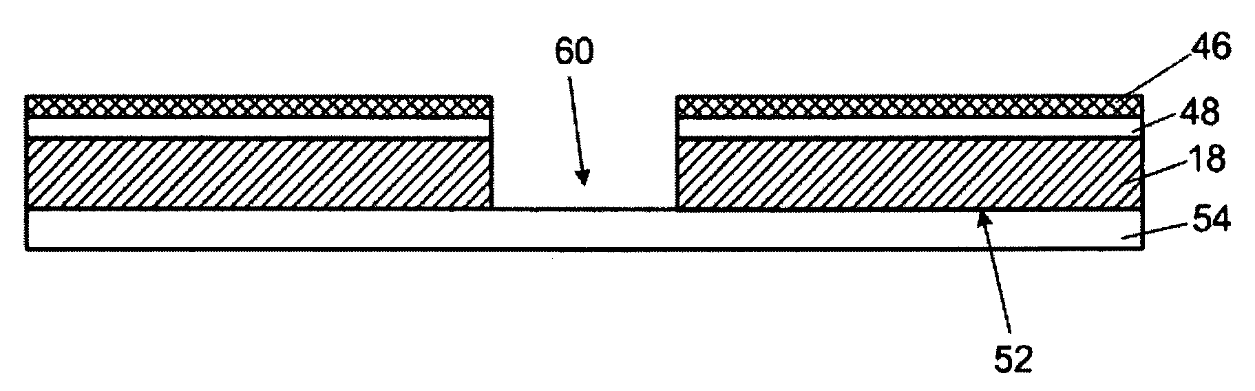
[0037]In a first embodiment, a readily soluble polymeric material such as a positive photoresist material, a polyhydroxy styrene material, a low molecular weight epoxy material, a styrene material, or an acrylate material is coated onto the opposite side 52 of the wafer 18 to serve as the relative soft etch stop layer 54 as shown in FIG. 5B. The soft etch stop layer 54 may be applied by a spin-coat process, a spray coat process, or a lamination process. Next, a hardcoat layer is 56 applied to the soft etch stop layer 54, such as by a method selected from sputtering, chemical vapor deposition (CVD), and spin on coating as shown in FIG. 5C. The hardcoat layer may be selected from, for example, silicon oxide, silicon nitride, silicon carbide or a combination thereof, diamond like carbon (DLC), a metal, a fluoropolymer passivation material deposited in a plasma chamber, for example, plasma deposition using octafluorocyclobutane as the monomer gas. The composite etch stop material 54 / 56 ...

second embodiment

[0039]In the second embodiment, the readily soluble polymeric material is coated onto the wafer 18 first to serve as a soft etch stop layer 54 while the highly cross-linked epoxy resin is coated onto the soft etch stop layer 54 to provide a hard etch stop layer 56. The thickness of the composite etch stop material 54 / 56 is controlled by controlling the weight percent solids in each of the polymer solutions as well as the spin coating speed used to apply the polymeric coatings to the surface 52 of the wafer 18 or to the soft etch stop layer 54. Typically, the composite etch stop material 54 / 56 will have an overall thickness T ranging from about 10 to about 25 microns with the soft etch stop layer 54 having a thickness ranging from about 5 to about 20 microns and the hard etch stop layer having a thickness ranging from about 1 to about 3 microns). In the alternative, the layers 54 and 56 may be selected from other negative or positive photoresist materials applied in a similar manner ...


PUM


Abstract

A process for etching semiconductor substrates using a deep reactive ion etching process to produce through holes or slots (hereinafter “slots”) in the substrates. The process includes applying a first layer to a back side of a substrate as a first etch stop material. The first layer is a relatively soft etch stop material. A second layer is applied to the first layer on the back side of the substrate to provide a composite etch stop layer. The second layer is a relatively hard etch stop material. The substrate is etched from a side opposite the back side of the substrate to provide a slot in the substrate.

Description

FIELD OF THE DISCLOSURE[0001]The disclosure relates to etching processes and in particular improvements in deep reactive ion etching processes.BACKGROUND AND SUMMARY[0002]During deep reactive ion etching (DRIE) of wafers of semiconductor substrate, the wafers are positioned and held in place on an electrostatic clamping disk. The clamping disk uses a DC power source to induce a charge on the surface of the wafer to be etched. The charge on the wafer provides an electrostatic force that pulls the wafer onto the clamping disk. As opposed to mechanical clamping, an electrostatic clamping mechanism increases a surface area of the wafer available for etching.[0003]The clamping disk also includes a cooling mechanism for cooling a back side of the wafer during the DRIE etching process. The cooling mechanism provides helium gas which flows through channels in the clamping disk to the back side of the wafer. Helium gas serves as a heat transfer medium between the wafer and the clamping disk....

Claims


Application Information

Patent Timeline
Patent Type & Authority Patents(United States)
IPC IPC(8): H01L21/302H01L21/461
CPCB81C1/00531B81C1/00619H01L21/0332H01L21/0334H01L21/3081H01L21/3083B81B2203/0353B81C2201/0132B81C2201/014
Inventor KRAWCZYK, JOHN W.MCNEES, ANDREW L.MONEY, CHRISTOPHER J.PATIL, GIRISH S.RHINE, DAVID B.VAIDEESWARAN, KARTHIK
Owner FUNAI ELECTRIC CO LTD
Why Eureka
Try Eureka