Semiconductor device including a multi-channel fin field effect transistor including protruding active portions and method of fabricating the same

a technology of fin field effect transistor and active portion, which is applied in the direction of transistors, semiconductor devices, electrical equipment, etc., can solve the problems of reducing the characteristics of the device as an active switch, degrading the effect and it is difficult to effectively suppress the influence of drain electrical potential on the source electrical potential and the channel. , to achieve the effect of increasing the current level of the transistor, increasing the effective channel length of the transistor, and increasing the current level

Active Publication Date: 2008-07-01
SAMSUNG ELECTRONICS CO LTD
View PDF5 Cites 94 Cited by
  • Summary
  • Abstract
  • Description
  • Claims
  • Application Information

AI Technical Summary

Benefits of technology

[0013]It is yet another feature of an embodiment of the present invention to provide a semiconductor device including a multi-channel FinFET and a method of fabricating the same that significantly increases an effective channel length of the transistor.
[0014]It is still another feature of an embodiment of the present invention to provide a semiconductor device including a multi-channel FinFET and a method of fabricating the same that is able to increase a current level of a transistor, thereby increasing an operating speed of the semiconductor device, by providing a plurality of fin-type active channels in the transistor.
[0015]It is yet still another feature of an embodiment of the present invention to provide a semiconductor device including a multi-channel FinFET and a method of fabricating the same that is able to produce a lower cost FinFET gate having a plurality of fin-type active channels using a simplified manufacturing process.

Problems solved by technology

This decrease in channel length, however, may degrade characteristics of the device as an active switch.
Thus, it becomes difficult to effectively suppress an influence of a drain electrical potential on a source electrical potential and a channel electrical potential.
However, since a conventional MOSFET, in which a channel is disposed parallel on a surface of a semiconductor, is a planar channel device, it is difficult to not only structurally scale down the MOSFET, but also to suppress the occurrence of the short channel effect.
Although the FinFET offers these superior electrical characteristics, it is currently difficult to make a FinFET having a very short and uniform channel width transistor, e.g., less than 30 nm, because of the limitations of current lithography techniques.
These limitations lead to other disadvantages.
For example, if fins are not formed to a uniform width, a current dispersion characteristic may be deteriorated.
However, a line width that can be obtained by the photolithography process is limited.
Thus, it is difficult to increase a contact region of a source and a drain due to the above-described patterning problems.

Method used


Image

  • Semiconductor device including a multi-channel fin field effect transistor including protruding active portions and method of fabricating the same
  • Semiconductor device including a multi-channel fin field effect transistor including protruding active portions and method of fabricating the same
  • Semiconductor device including a multi-channel fin field effect transistor including protruding active portions and method of fabricating the same

Examples


first through fourth embodiments

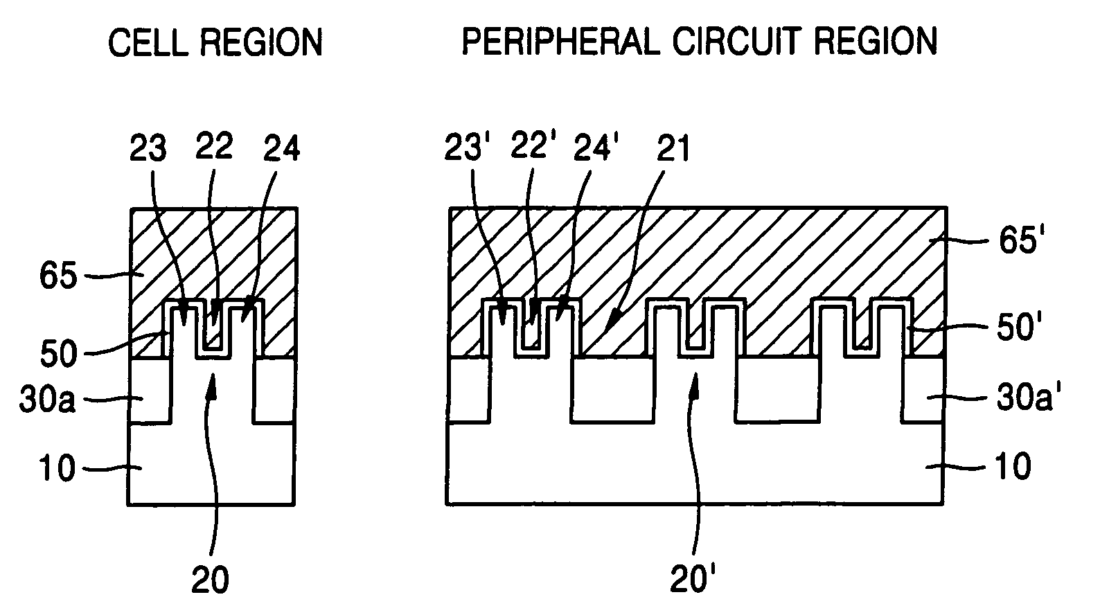
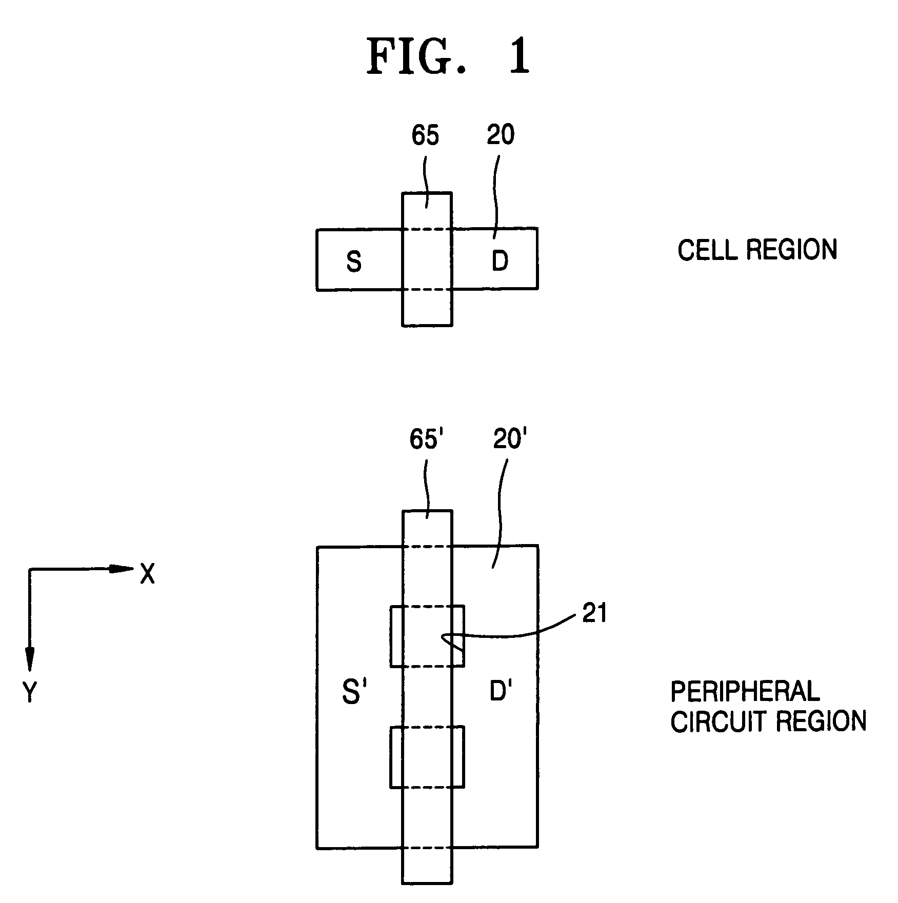
[0047]FIG. 1 illustrates a plan view of a semiconductor device formed by a method of fabricating a semiconductor device according to a first through fourth embodiment of the present invention.

[0048]Referring to FIG. 1, a semiconductor device is divided into a cell region and a peripheral circuit region. The cell region includes an active region 20 and a gate electrode 65. The active region 20 and the gate electrode 65, which is formed on the active region 20, are perpendicular relative to one another. For example, a length of the active region 20 may extend in an x-direction and a length of the gate electrode 65 may extend in a y-direction. The active region 20 includes a source S and a drain D formed on either side of the gate electrode 65.

[0049]The peripheral circuit region includes an active region 20′ and a gate electrode 65′, which is formed on the active region 20′. The active region 20′ and the gate electrode 65′ are both substantially rectangular in shape. A length of the ga...

first embodiment

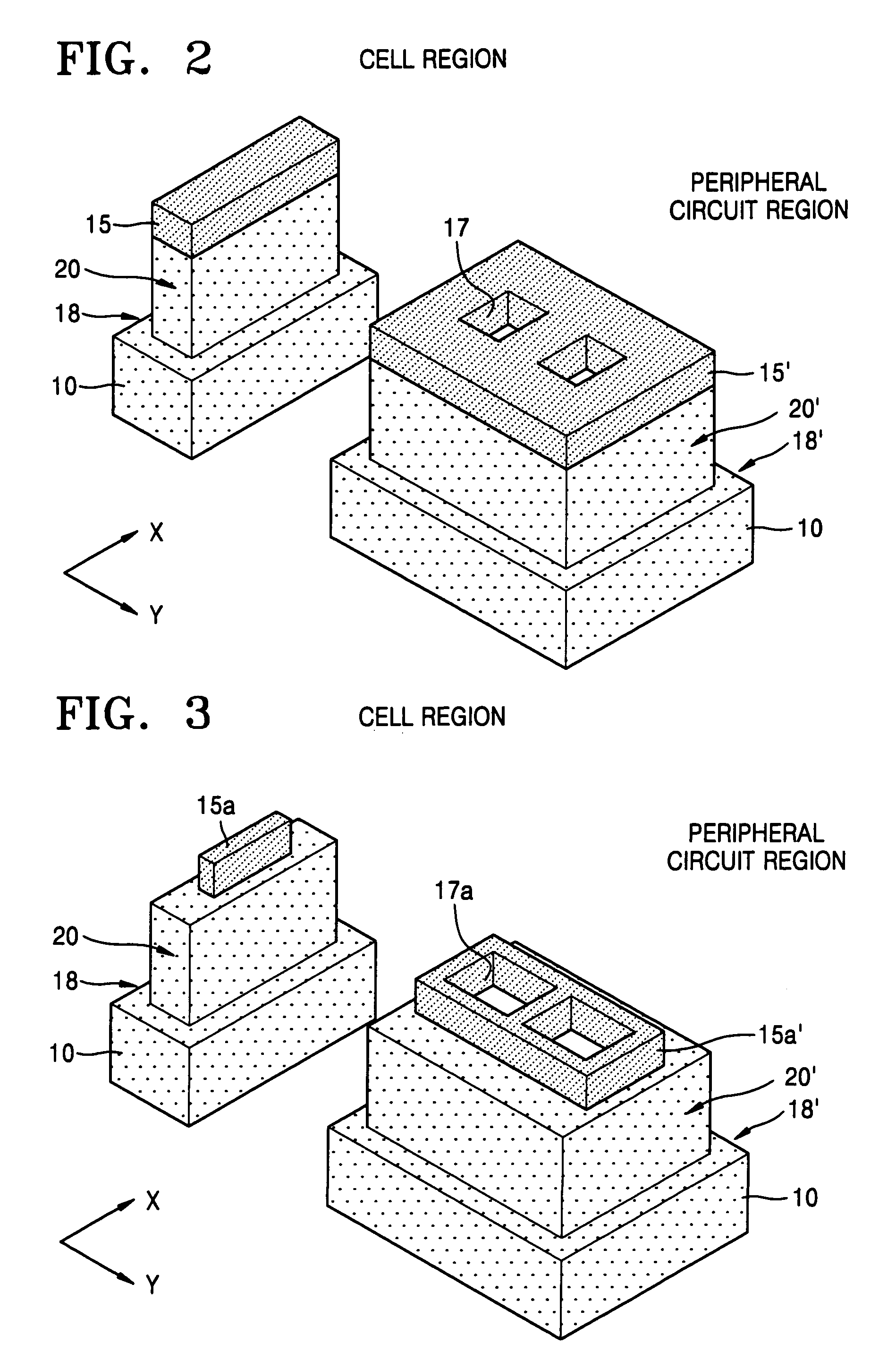
[0053]FIGS. 2 through 9 illustrate perspective views of stages in a method of fabricating a semiconductor device in accordance with a first embodiment of the present invention.

[0054]Referring to FIG. 2, hard mask layers 15 and 15′ are deposited on a semiconductor substrate 10. Subsequently, the hard mask layers 15 and 15′ will be patterned to define active regions 20 and 20′ of the semiconductor substrate 10. The semiconductor substrate 10 may be a bulk silicon wafer, a silicon-on-insulator (SOI) substrate, a silicon germanium-on-insulator (SGOI) substrate, or a silicon germanium (SiGe) wafer. The hard mask layers 15 and 15′ may be formed simultaneously in both the cell region and the peripheral circuit region.

[0055]To form the hard mask layers 15 and 15′, an insulating layer, such as a silicon nitride layer, is deposited on the substrate 10 to a thickness of about 800 to 2000 Å, and is patterned along the cell region and the peripheral circuit region to form predetermined shapes. T...

second embodiment

[0082]FIGS. 11A and 11B illustrate cross-sectional views, taken along the y-direction, of a semiconductor device in accordance with a second embodiment of the present invention and a semiconductor device in accordance with an alternative second embodiment of the present invention, respectively.

[0083]A method of fabricating a semiconductor device according to either the second or alternative second embodiment of the present invention is substantially similar to the method of fabricating a semiconductor device according to the first embodiment of the present invention. More specifically, the methods only differ with respect to the operation described above in connection with FIGS. 7 and 8. More specifically, when the operation described in connection with FIG. 7 is performed in the method of the second embodiment, the substrate 10 disposed under openings 45 and 45′ is etched to a greater depth than in the first embodiment to define portions of the active regions 20 and 20′ to be used ...


PUM


Abstract

In a semiconductor device, and a method of fabricating the same, the semiconductor device includes a semiconductor substrate having a cell region and a peripheral circuit region, a portion of the semiconductor substrate in the cell region and in the peripheral circuit region including an isolation region defining an active region, a portion of the active region protruding above an upper surface of the isolation region to define at least two active channels, a gate dielectric layer formed over the active region of the semiconductor substrate including the at least two protruding active channels, a gate electrode formed over the gate dielectric layer and the isolation region of the semiconductor substrate, and a source / drain region formed in the active region of the semiconductor substrate on either side of the gate electrode.

Description

BACKGROUND OF THE INVENTION[0001]1. Field of the Invention[0002]The present invention relates to a semiconductor device including a multi-channel fin field effect transistor (FinFET) and a method of fabricating the same. More particularly, the present invention relates to a semiconductor device including a multi-channel FinFET in a cell and / or peripheral circuit region of a semiconductor substrate and a method of fabricating the same.[0003]2. Description of the Related Art[0004]In order to improve performance and reduce fabrication cost of semiconductor devices, an integration density of semiconductor devices must continually increase. Increasing integration density of semiconductor devices requires developing techniques for reducing a feature size of a semiconductor device.[0005]In conventional semiconductor fabricating processes, the channel length of a metal-oxide-semiconductor field effect transistor (MOSFET) is decreased to increase an operating speed and integration density of...

Claims


Application Information

Patent Timeline
Patent Type & Authority Patents(United States)
IPC IPC(8): H01L29/76H01L29/745H01L21/336H01L21/84H01L27/12H01L29/78H01L29/786
CPCH01L21/84H01L27/1203H01L29/66795H01L29/785H01L29/66545H01L29/78684H01L21/18
Inventor KIM, SUNGMINPARK, DONGGUNYOON, EUNJUNGJANG, SEMYEONGKIM, KEUNNAMOH, YONGCHUL
Owner SAMSUNG ELECTRONICS CO LTD
Why Eureka
Try Eureka