

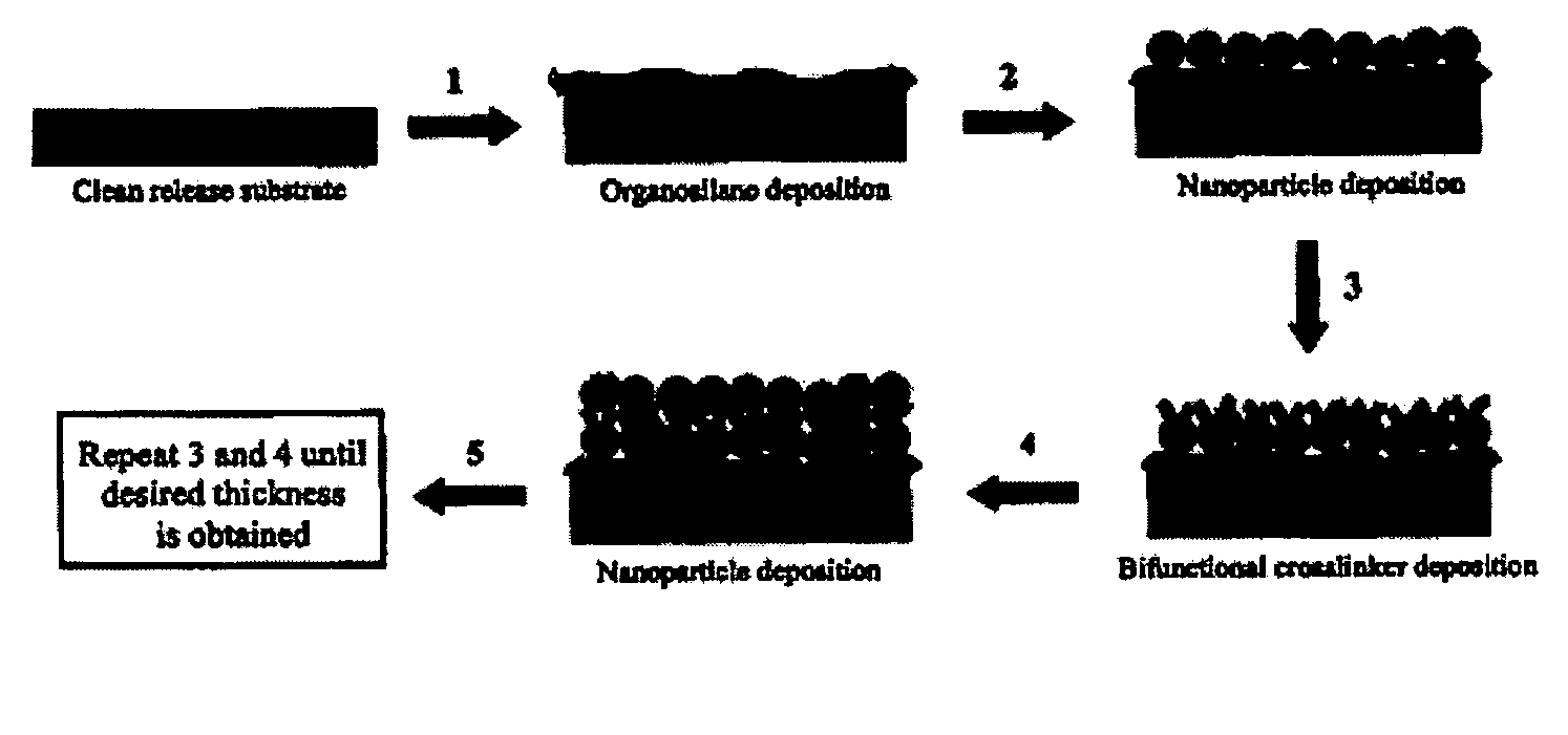
Rapidly self-assembled thin films and functional decals
a technology of nanoparticles and functional decals, which is applied in the direction of thin material processing, material nanotechnology, coatings, etc., can solve the problems of large manufacturing facilities that are expensive to build and operate, the fabrication process typically used to create electronic and electromechanical components is often harsh, and the self-assembly process is highly advantageous. , to achieve the effect of high reproducibility, simple operation and cost-effectiveness
- Summary
- Abstract
- Description
- Claims
- Application Information
AI Technical Summary
Benefits of technology
Problems solved by technology
Method used
Image

Examples
example 1
Resins for Reaction with Self Assembled Nanoparticles
[0076]A series of polysiloxanes were synthesized that contain both a controlled number of reactive sites available for both bonding to ceramic (e.g. Al2O3) nanoparticles and for crosslinking reactions. Novel polysiloxanes offer excellent weatherability including degradation resistance against ozone and UV. Lower stress adhesive nanocomposites based on polysiloxanes also minimize debonding affects that result when bonding substrates with highly mismatched coefficients of thermal expansion. Polyorganosiloxanes are also known for their high flexibility over a wide service temperature range. Such networks would remain flexible under cryogenic conditions and perform consistently mechanically above 250° C. Polyorganosiloxanes with pendent quaternized phosphine, phosphine oxide, and nitrile moieties are known to complex with oxide and metal nanoparticles with hydroxyl rich surfaces.
[0077]Polysioxanes with pendent carboxylic acid moieties...
example 2
Electrically Conducting Elastomeric Material
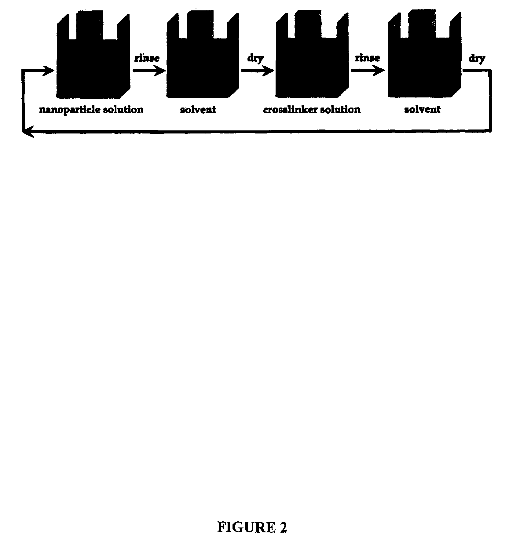
[0083]The formation of a free-standing, mechanically robust, low modulus, electrically-conducting material is described in this example. This material comprised gold nanoparticles, a poly(etherurethane)polymer, mercaptoethanol as the crosslinker, 3-mercaprtopropyltriethoxysilane as the primer and polycarbonate as the substrate.
[0084]Following functionalizing the substrate with 3-mercaptopropyltriethoxysilane, the functionalized substrate was (1) immersed into a naked colloidal gold solution for approximately 1 to 120 minutes (preferable 60 minutes), rinsed in ultra pure water, (2) dipped into an aqueous solution of mercaptoethanol for approximately 1 to 30 minutes (specifically 10 minutes), rinsed in ultra pure water and (3) immersed into a poly(etherurethane)polymer solution for about 1 to 120 minutes (specifically 60 minutes), rinsed and then dried. The sequential immersion was repeated until a buildup of 52 bilayers and a material thick...
example 3
Thermally Conductive Elastomeric Material
[0086]The formation of a free-standing, mechanically robust, low modulus thermally-conducting material is described in this example. The fabrication of this material followed the approach as described in Example 1. This material comprised silver nanoparticles and poly(dimethyl-co-methylhydrido-co-3-cyanopropryl,methyl)siloxane as the polymer.
[0087]First the polycarbonate substrate was functionalized by immersing the substrate in a solution containing 3-aminopropyltrimethoxysilane. Next, the functionalized substrate was immersed into a colloid silver solution for approximately 1 to 120 minutes (specifically 60 minutes), rinsed in ultra pure water, and then dipped into a poly(dimethyl-co-methylhydrido-co-3-cyanopropryl,methyl)siloxane solution for approximately 1 to 120 minutes (specifically 60 minutes), rinsed in ultra-pure water and then dried. This immersion cycle was repeated until a buildup of 31 bilayers and a material thickness of about ...
PUM
| Property | Measurement | Unit |
|---|---|---|
| diameter | aaaaa | aaaaa |
| thickness | aaaaa | aaaaa |
| electrical bulk conductivity | aaaaa | aaaaa |
Abstract
Description
Claims
Application Information