Anneal of epitaxial layer in a semiconductor device

a semiconductor and epitaxial layer technology, applied in the direction of polycrystalline material growth, crystal growth process, gel state, etc., can solve the problems of material thermal instability, carbon-doped silicon layer epitaxially grown on a silicon layer may be under stress due to lattice constant mismatch,

Inactive Publication Date: 2008-08-26
NORTH STAR INNOVATIONS
View PDF8 Cites 109 Cited by
  • Summary
  • Abstract
  • Description
  • Claims
  • Application Information

AI Technical Summary

Problems solved by technology

The addition of tin or carbon to a silicon or germanium layer may present difficulties due to relatively large lattice mismatches and phase diagram differences.
Accordingly, a carbon-doped silicon layer epitaxially grown on a silicon layer may be under stress due to lattice constant mismatch.
One problem with epitaxial silicon carbon (or other layers having carbon) is that the material is thermally unstable.
Accordingly, by annealing the layer at a high temperature, the strain of an epitaxially grown silicon carbon alloy layer may undesirably decrease.

Method used


Image

  • Anneal of epitaxial layer in a semiconductor device
  • Anneal of epitaxial layer in a semiconductor device
  • Anneal of epitaxial layer in a semiconductor device

Examples


Embodiment Construction

[0013]The following sets forth a detailed description of a mode for carrying out the invention. The description is intended to be illustrative of the invention and should not be taken to be limiting.

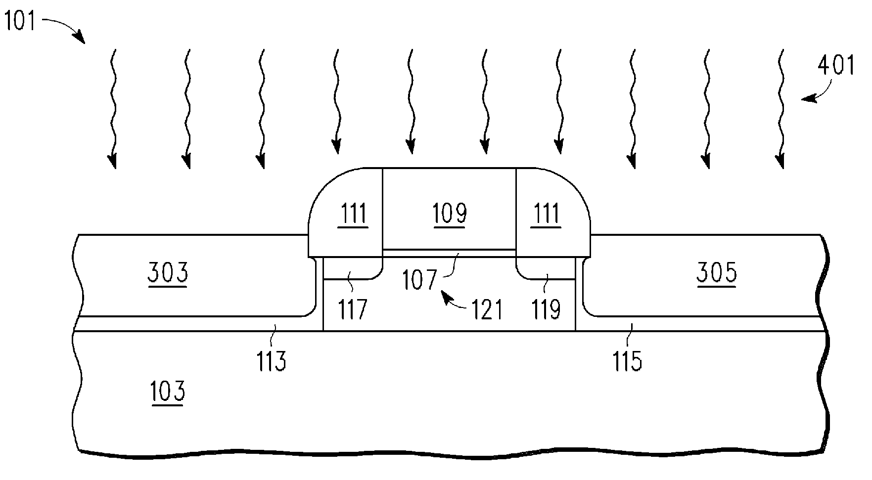
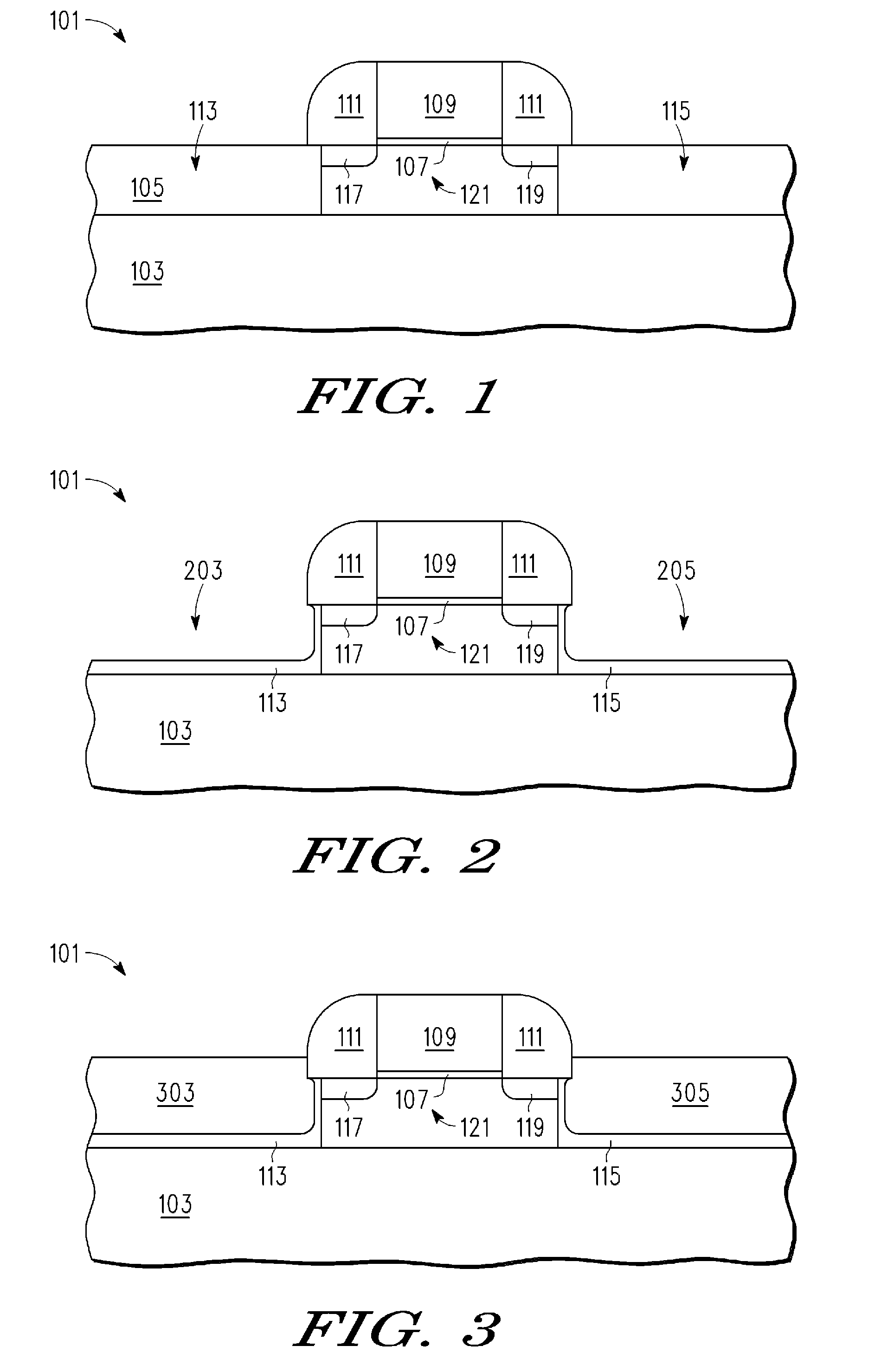
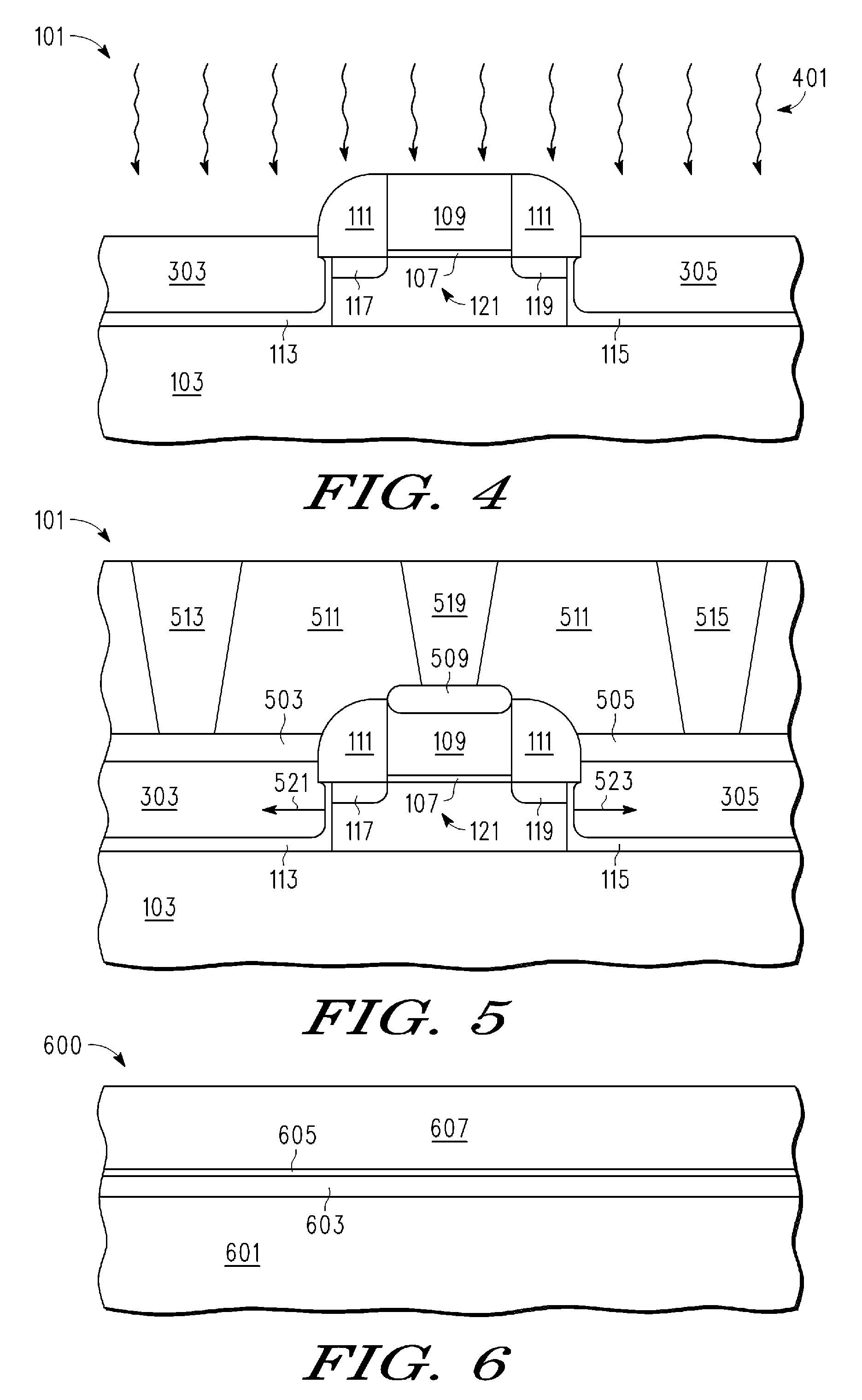
[0014]FIG. 1 is a cutaway side view of one embodiment of a semiconductor device at one stage of its manufacture according to one embodiment of the present invention. Wafer 101 has a semiconductor on insulator (SOI) configuration that includes a semiconductor layer 105 (e.g. silicon) located on insulator layer 103. In one embodiment, layer 103 would be located on a bulk silicon substrate layer (not shown). Layer 105 has been implanted with dopants to form channel region 121 and lightly doped source / drain implant regions 117 and 119 and heavily doped source / drain implant regions 113 and 115. A gate 109 (e.g. polysilicon, metal) is formed over a gate dielectric 107 (e.g. SiO2 or metal oxides such as hafnium or zirconium based). A dielectric gate spacer 111 is formed adjacent to gate 109. In...


PUM

PropertyMeasurementUnit
temperatureaaaaaaaaaa
lattice spacingaaaaaaaaaa

Abstract

An anneal of an epitaxially grown crystalline semiconductor layer comprising a combination of group-IV elements. The layer contains at least one of the group of carbon and tin. The layer of epitaxially grown material is annealed at a temperature substantially in a range of 1,000 to 1,400 degrees Celsius for a period not to exceed 100 milliseconds within 10% of the peak temperature. The anneal is performed for example with a laser anneal or a flash lamp anneal. The limited-time anneal may improve carrier mobility of a transistor.

Description

BACKGROUND OF THE INVENTION[0001]1. Field of the Invention[0002]This invention relates in general to semiconductor devices and more specifically to annealing an epitaxial layer in a semiconductor device.[0003]2. Description of the Related Art[0004]Semiconductor devices utilize epitaxially grown material that includes carbon or tin. Examples of such materials include alloys containing two or more of silicon, germanium, carbon, and tin. The addition of tin or carbon to a silicon or germanium layer may present difficulties due to relatively large lattice mismatches and phase diagram differences. For example, a silicon lattice has a spacing of 5.43 Angstroms and a germanium lattice has a spacing of 5.65 Angstroms. Tin has a lattice spacing of 6.49 Angstroms and diamond carbon has a lattice spacing of 3.57 Angstroms.[0005]The lattice constant of relaxed carbon-doped silicon is smaller than that of silicon. Accordingly, a carbon-doped silicon layer epitaxially grown on a silicon layer may...

Claims


Application Information

Patent Timeline
Patent Type & Authority Patents(United States)
IPC IPC(8): C30B25/14C30B25/12
CPCH01L29/1054H01L29/7848H01L29/7834H01L29/66636H01L29/665
Inventor ZOLLNER, STEFANDHANDAPANI, VEERARAGHAVANGRUDOWSKI, PAUL A.SPENCER, GREGORY S.
Owner NORTH STAR INNOVATIONS
Why Eureka
Try Eureka