Liquid crystal display device and method for manufacturing the same

a liquid crystal display and liquid crystal technology, applied in non-linear optics, instruments, optics, etc., can solve the problems of difficult liquid crystal injection, high manufacturing cost, and high cost of liquid crystal material interposed between pixel electrodes and opposing electrodes, so as to prevent deterioration, high reliability, and high reliability

Inactive Publication Date: 2008-09-16
SEMICON ENERGY LAB CO LTD
View PDF50 Cites 22 Cited by
  • Summary
  • Abstract
  • Description
  • Claims
  • Application Information

AI Technical Summary

Benefits of technology

[0017]In addition, the sealant may be drawn by a dispenser device or an ink jet device. Further, the sealant may be drawn under reduced pressure or in inert atmosphere at atmospheric pressure. In case that solvent is added to the sealant for controlling the degree of viscosity, the solvent, which is hardly volatile, is preferably used to prevent the sealant from deteriorating and curing during dropping under reduced pressure.
[0053]According to the invention, a high reliable liquid crystal display device, which uses liquid crystal materials efficiently, and which has flexibility, becomes possible to be mass-produced.

Problems solved by technology

Manufacturing cost is increased with the increasing of a panel size.
Especially, the liquid crystal material interposed between a pixel electrode and an opposing electrode is expensive.
Especially, in case of a large sized panel, it becomes difficult to inject a liquid crystal by a capillary phenomenon and to fill the region (at least including a pixel portion) surrounded by seal with the liquid crystal.
There is the threat that since extremely larger amounts of liquid crystal passes the path of the liquid crystal extended from the liquid crystal inlet to the pixel region, especially, the vicinity of the liquid crystal inlet, compared with another region of the panel; the surface of an orientation film is deteriorated due to friction caused by injecting the liquid crystal, and a liquid crystal orientation is distorted as a result.
However, these substrates have disadvantages of being fragile and heavy.
Further, the glass substrate or the quartz substrate is unsuited to mass-production since it is difficult to use a large sized glass or quartz substrate for mass-production.
However, a plastic film has poor blocking properties against impurities such as moisture or alkaline metals, so that a high reliable liquid crystal display device cannot be obtained.
Consequently, a liquid crystal display device having high technical advantages, which is manufactured by using a plastic substrate, has not been realized yet.

Method used


Image

  • Liquid crystal display device and method for manufacturing the same
  • Liquid crystal display device and method for manufacturing the same
  • Liquid crystal display device and method for manufacturing the same

Examples


embodiment mode 1

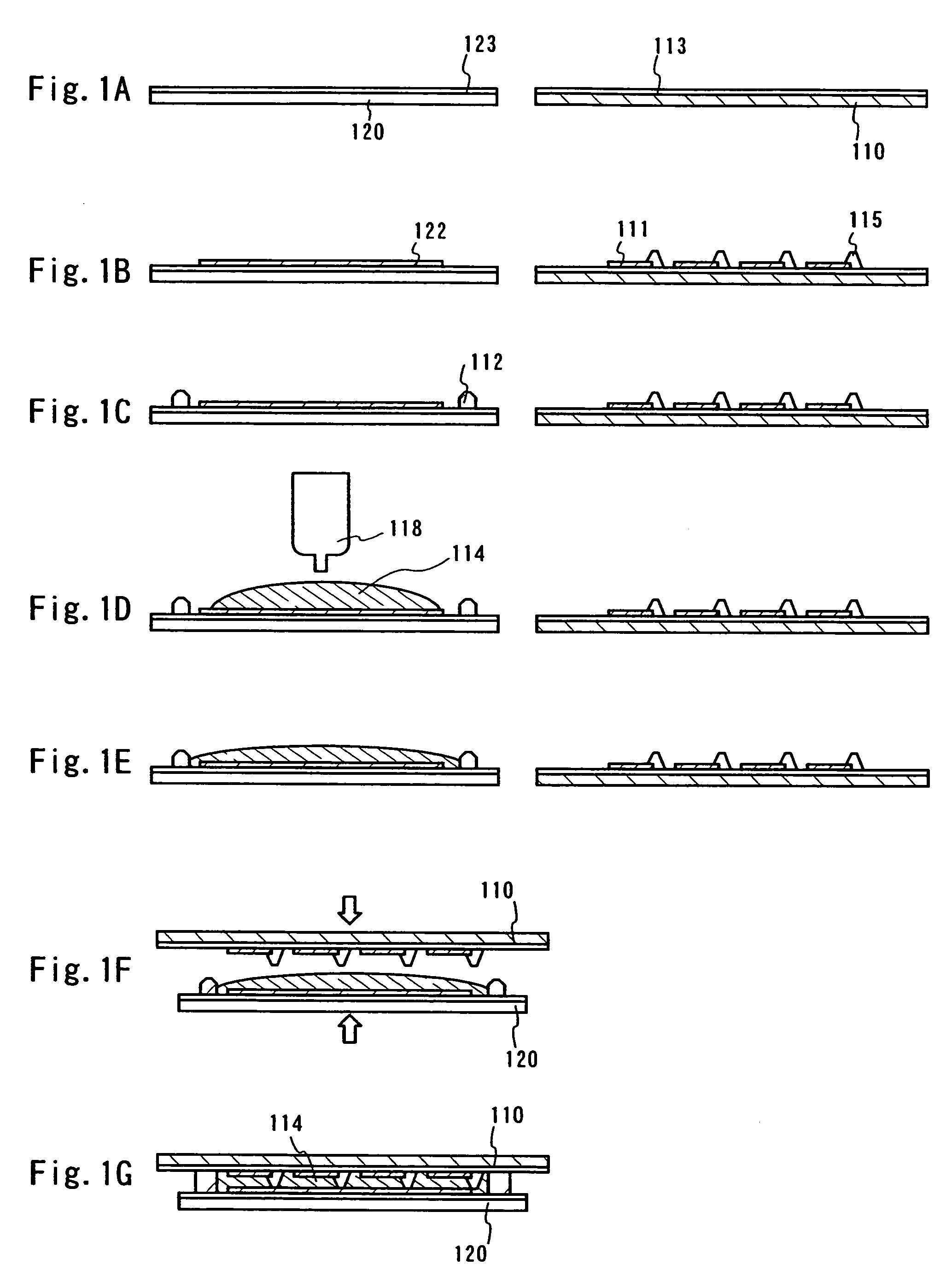
[0068]A second substrate 120, which serves as an opposing substrate, and a first substrate 110, which is preliminarily provided with a TFT (not shown) are prepared. The first substrate 110 and the second substrate 120 are especially not limited if they only have flexibility and are transparent to light. Typically, a plastic substrate is used for the substrates. As the TFT, any one of the following may be used: a TFT, which uses polysilicon as an active layer (also referred to as a polysilicon TFT); a TFT, which uses amorphous silicon as an active layer (also referred to as an amorphous silicon TFT); or a TFT, which uses an organic semiconductor material as an active layer (also referred to as an organic TFT).

[0069]A plastic substrate has advantages of lightweight and thin film thickness, however, the plastic substrate has poor blocking properties against moisture. Subsequently, a protective film is formed over either or both surfaces of the plastic substrate in the present invention...

embodiment mode 2

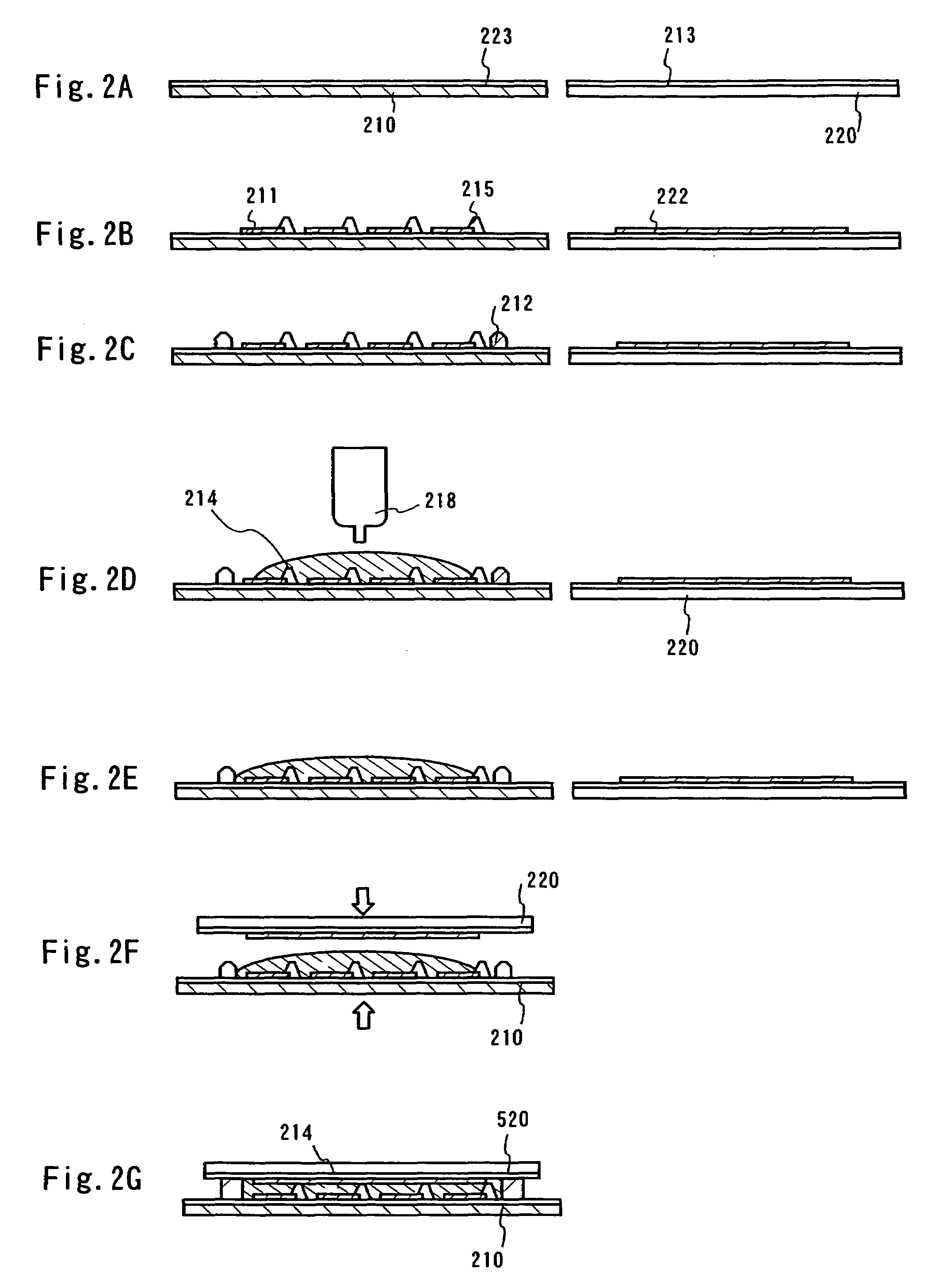
[0080]An example of drawing sealant and dropping liquid crystal on the TFT substrate side will be explained hereinafter.

[0081]As in Embodiment Mode 1, a second substrate 220, which serves as an opposing substrate, and a first substrate 210, which is provided with a TFT (not shown) are prepared. The first substrate 210 and the second substrate 220 are especially not limited if they only have flexibility and are transparent to light. Typically, a plastic substrate is used for the substrates.

[0082]Then, as in Embodiment Mode 1, a protective film 213 is formed over the second substrate 220, which serves as an opposing substrate, and a protective film 223 is formed over the first substrate 210 (FIG. 2A). Although a TFT or the like over the first substrate are not shown in the drawings, the first substrate is provided with at least the silicon nitride film as a base insulating film, an interlayer insulating film, or a protective film of the TFT.

[0083]And then, a pixel electrode 211 formed...

embodiment 1

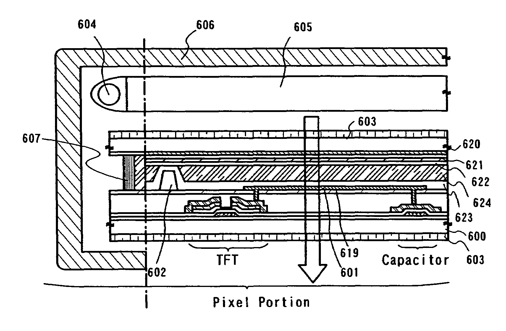
[0101]In this embodiment, a process for manufacturing an active matrix liquid crystal display device will be described hereinafter with reference to FIG. 7.

[0102]First, an active matrix substrate is formed by using a substrate 600, which is transparent to light. A substrate having a large size of 600 mm×720 mm, 680 mm×880 mm, 1000 mm×1200 mm, 1100 mm×1250 mm, 1150 mm×1300 mm, 1500 mm×1800 mm, 1800 mm×2000 mm, 2000 mm×2100 mm, 2200 mm×2600 mm, or 2600 mm×3100 mm is preferably used in order to reduce manufacturing costs. As a usable substrate, a barium borosilicate glass, an aluminoborosilicate glass, and the like, as typified by #7059 glass or #1737 glass produced by Corning Inc. can be used. Besides, a transparent substrate such as a quartz substrate or a plastic substrate can be also used.

[0103]After a conductive film is deposited by sputtering over a whole surface of the substrate 600 having an insulating surface, a first process of photolithography is carried out to form a resist...


PUM

PropertyMeasurementUnit
sizeaaaaaaaaaa
sizeaaaaaaaaaa
sizeaaaaaaaaaa

Abstract

A liquid crystal display device using a plastic substrate becomes required to have high resolution, high opening ratio, high reliability, or the like, with the increasing of a screen size. Besides, high productivity and cost reduction is also required. According to the present invention, a protective film 123 comprising at least one silicon nitride film, which is formed by a ratio frequency sputtering using a silicon target, is provided over an opposing substrate (a flexible substrate); sealant 112 is drawn; a liquid crystal material 114 is dropped over the opposing substrate in vacuo; and the opposing substrate is pasted to a flexible substrate 110 provided with a pixel electrode 111 and a columnar spacer 115.

Description

BACKGROUND OF THE INVENTION[0001]1. Field of the Invention[0002]The present invention relates to a liquid crystal display device and a method for manufacturing the liquid crystal display device. More specifically, the invention relates to electronic equipment installed with an electro-optic device, which is typified by a liquid crystal display panel having circuits composed of thin film transistors (hereinafter, TFTs), and such electro-optic devices as components.[0003]2. Related Art[0004]In recent years, a technique for forming a TFT by a semiconductor thin film (having a thickness of approximately from several to several hundreds nm), which is formed over a substrate having an insulating surface. TFTs are applied broadly to electronic devices such as an IC or an electro-optic device, and has been rushed to be developed especially as a switching element of an image display device.[0005]A liquid crystal display device has been known as an image display device. An active matrix liqui...

Claims


Application Information

Patent Timeline
Patent Type & Authority Patents(United States)
IPC IPC(8): G02F1/13G02F1/1333G02F1/1341
CPCG02F1/1341G02F1/1339G02F2001/13415G02F1/13392G02F2202/02G02F1/13398G02F1/13415G02F1/13
Inventor YAMAZAKI, SHUNPEITAKAYAMA, TORU
Owner SEMICON ENERGY LAB CO LTD
Why Eureka
Try Eureka