

Printed wiring board manufacturing method
a manufacturing method and printed technology, applied in the direction of photomechanical equipment, non-metallic protective coating applications, instruments, etc., can solve the problems of deterioration of flexibility and bendability, weight increase, out of position, etc., to improve conductive reliability, avoid conductive defects in patterning, and improve conductive reliability
- Summary
- Abstract
- Description
- Claims
- Application Information
AI Technical Summary
Benefits of technology
Problems solved by technology
Method used
Image

Examples
Embodiment Construction
>
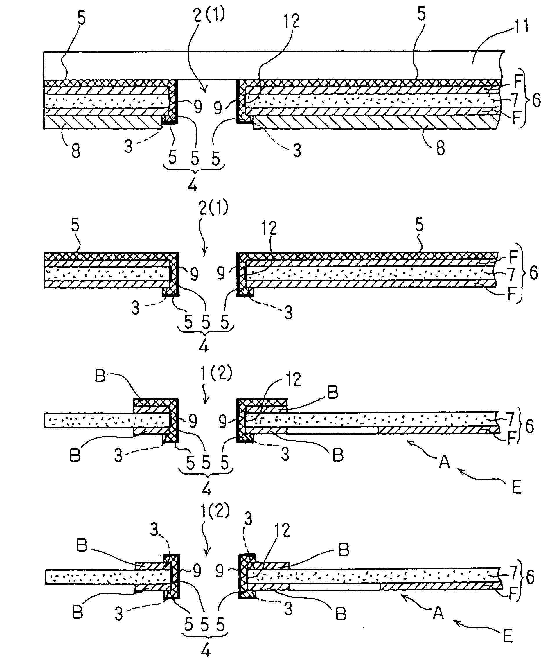
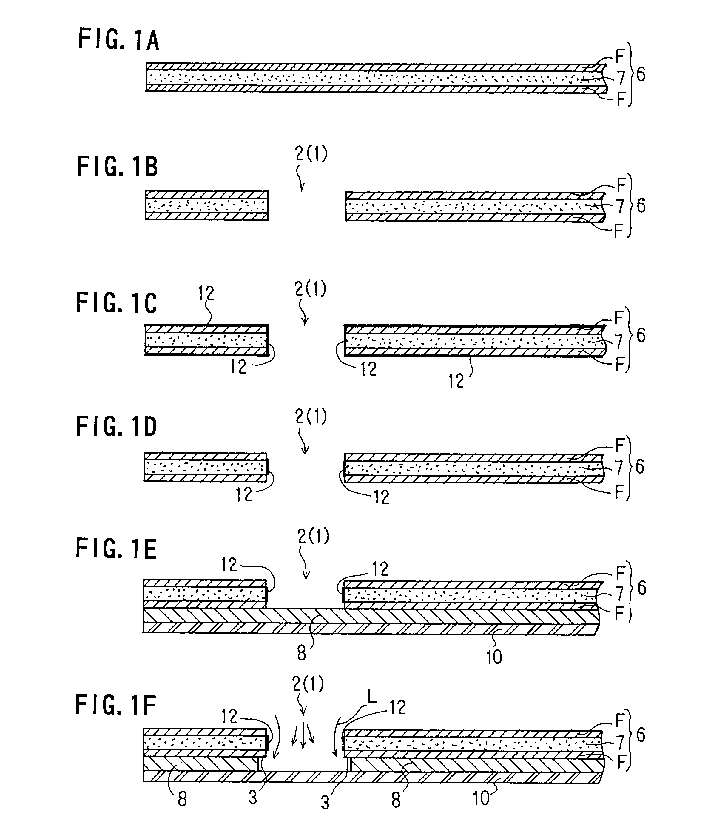
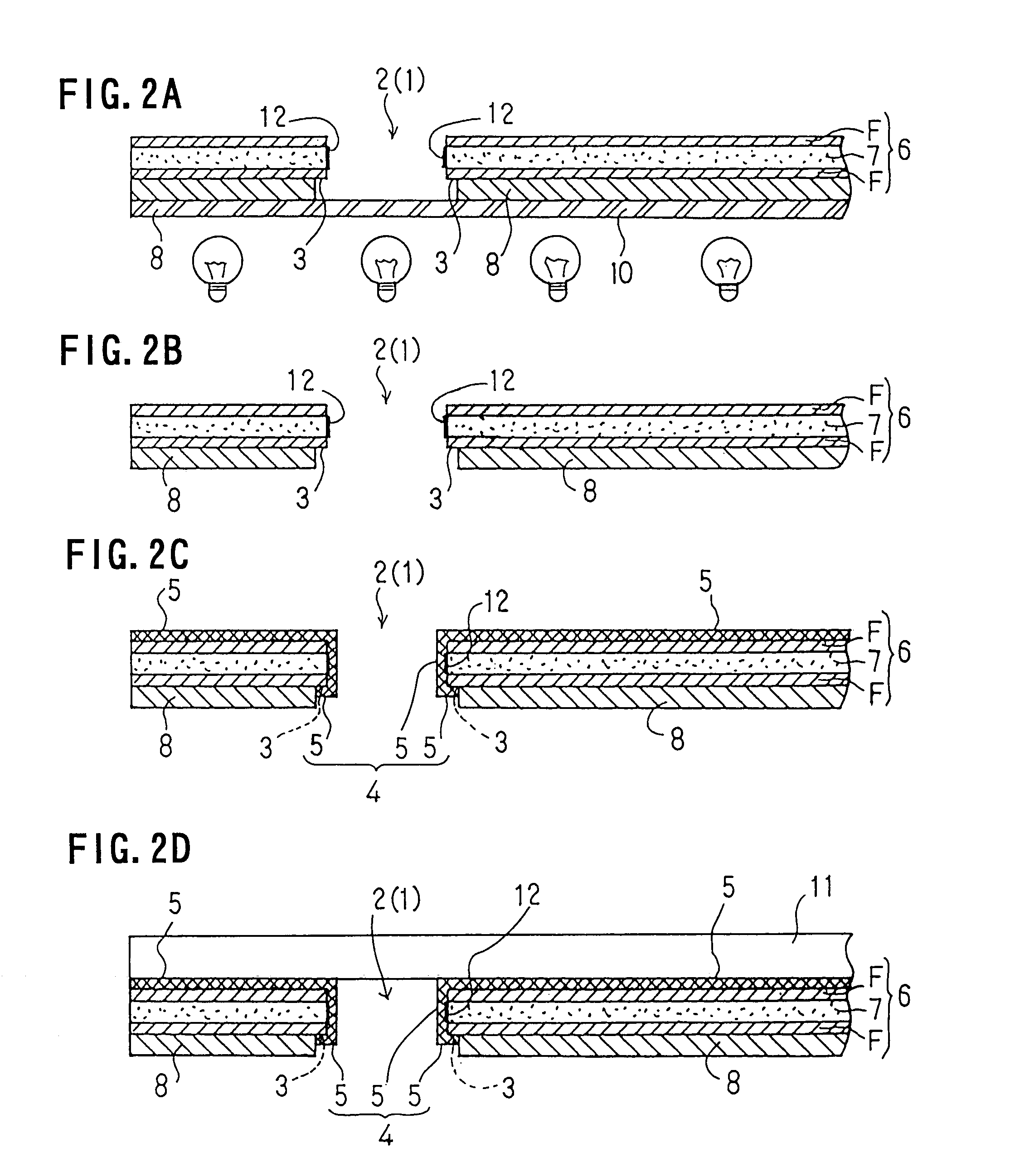
[0067]A printed wiring board E will be explained with reference to FIG. 8. The printed wiring board E is broadly classified into a flexible printed wiring board and a rigid printed wiring board. Each board is provided in such a manner that a circuit pattern A is formed as a conducting layer on one side or both sides of an outer surface of an insulating material 7.
[0068]The flexible printed wiring board is made of an insulating material 7, such as a polyimide film, of which the base material is flexible. In many cases, the circuit pattern A is formed on both sides (i.e., both front and rear side, in other words, both one side and the other side) of the insulating material 7.
[0069]On the other hand, the rigid printed wiring board is made of an insulating material 7, serving as a base material, such as a glass epoxy resin, a glass cloth and a ceramic, wherein the circuit pattern A is formed on one side (one of the front and rear sides) of the insulating material 7 or on both sides the...
PUM
| Property | Measurement | Unit |
|---|---|---|
| thickness | aaaaa | aaaaa |
| thickness | aaaaa | aaaaa |
| thickness | aaaaa | aaaaa |
Abstract
Description
Claims
Application Information