Single chip, noise-resistant, one-dimensional, CMOS sensor for target imaging

a target imaging and one-dimensional technology, applied in the field of noise-resistant imaging sensors, can solve the problems of large, overall size of the ccd sensor, more total power consumption, etc., and achieve the effect of reducing cost and size, and reducing power consumption

Active Publication Date: 2008-11-04
SYMBOL TECH LLC
View PDF10 Cites 15 Cited by
  • Summary
  • Abstract
  • Description
  • Claims
  • Application Information

AI Technical Summary

Benefits of technology

[0006]Accordingly, it is a general object of this invention to reduce power consumption, and to reduce cost and size, of an image sensor for use in an electro-optical reader for reading one-dimensional bar code symbols.
[0009]It is yet another object of the present invention to render handheld readers less susceptible to short battery lifetimes and bulkiness.
[0010]A still further object of the present invention is to suppress electrical noise generated when all the support circuitries are integrated on a single CMOS-based chip.FEATURES OF THE INVENTION
[0012]The use of CMOS technology allows integration of the analog front end, the digital back end, as well as other circuits, as described below, and achieves the advantages of reduced overall system size and cost, faster read-out speed of the information, and lower power consumption. However, these advantages come at the expense of high system noise and is a primary factor as to why CMOS technology has not heretofore been used for imaging symbols, especially bar code symbols. The overall system noise can come from a myriad of sources, such as white noise, dark current and fixed-pattern noise, all of which are inherent in the choice of sensor, as well as device electronic noise generated within electrical components and includes thermal noise generated by random thermally induced electron motion and flicker noise caused by crystal manufacturing defects and contaminants in the electrical components, interference noise generated from the environment and includes supply voltage noise, cross-talk noise and substrate noise, especially that caused by coupling between the analog front end and the digital back end, reset noise (also called KTC noise which is caused by the thermo-dynamic uncertainty of the number of charges on a capacitor) generated during resetting of the sensors and shot noise associated with the random arrival of photons at any sensor. The fixed-pattern noise is caused by system variations and non-uniformities in the pixels.
[0015]Other means for suppressing noise include the selection and design of a photodiode to have high quantum efficiency and low dark current, the placement of a high gain amplifier in each pixel immediately after the photodiode, and the use of an ADC for each photodiode so as to convert the analog signal to the digital signal as early as possible in the signal processing.

Problems solved by technology

The use of several support chips results in more total power consumption and a large, overall size for the CCD sensor.

Method used


Image

  • Single chip, noise-resistant, one-dimensional, CMOS sensor for target imaging
  • Single chip, noise-resistant, one-dimensional, CMOS sensor for target imaging
  • Single chip, noise-resistant, one-dimensional, CMOS sensor for target imaging

Examples


Embodiment Construction

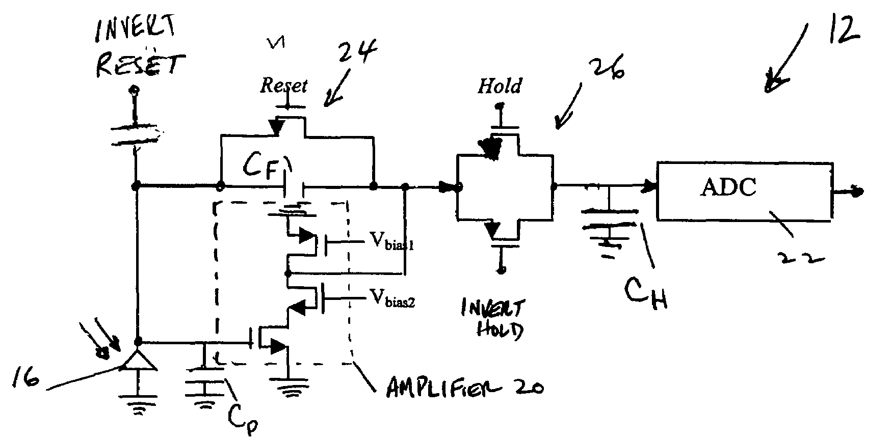
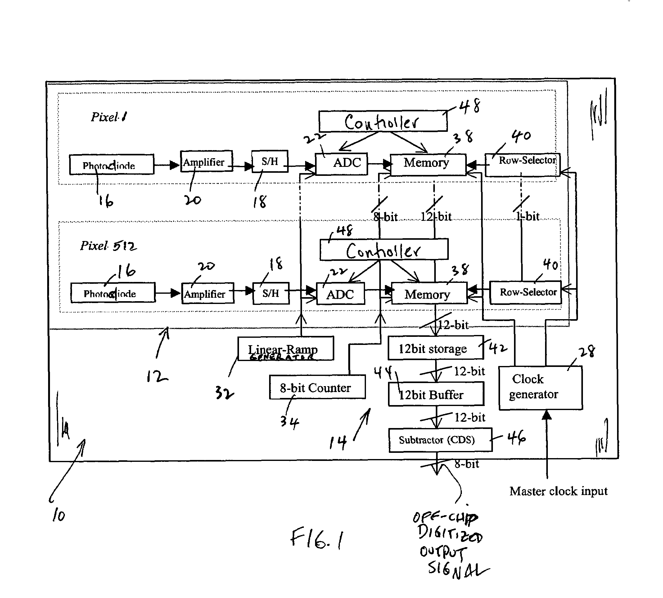
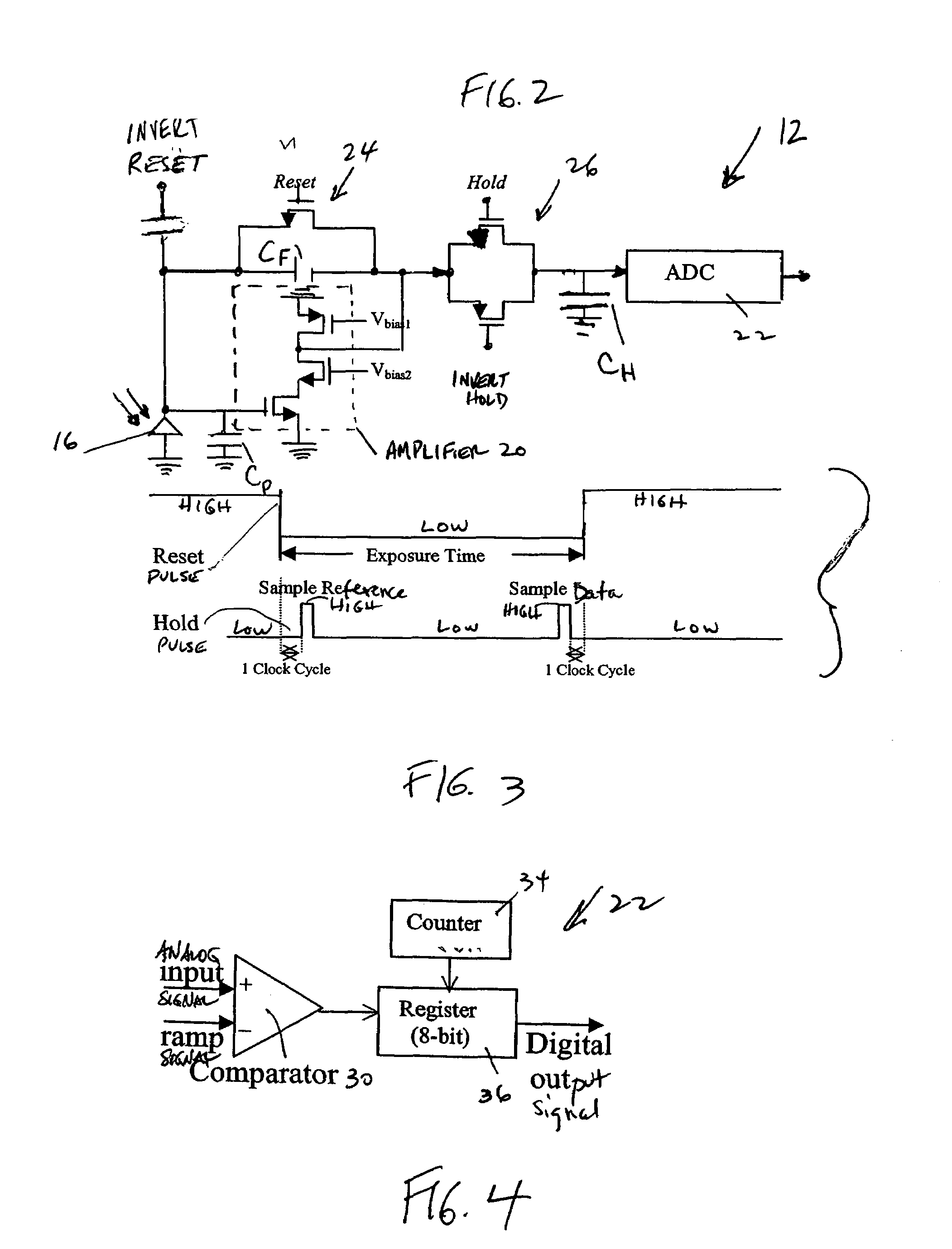
[0022]Referring to FIG. 1, reference numeral 10 generally identifies a single, solid-state, complementary metal-oxide semiconductor (CMOS) chip having an analog front end 12 and a digital back end 14, both the front and back ends being integrated on the same, single CMOS chip 10. The chip is used for imaging a target, especially a one-dimensional coded symbol such as a Universal Product Code (UPC) symbol.

[0023]The front end 12 includes a linear array of pixels, preferably 512 to 4096 pixels in all. Each pixel includes a photodiode 16, a sample-and-hold (S / H) circuit 18, a high gain amplifier 20, and an analog-to-digital converter (ADC) 22 which are shown in detail in FIG. 2. All the other components in FIG. 1 are part of the digital back end.

[0024]The photodiode 16 converts incident light into an electrical analog signal. The photodiode has a lower white noise, dark current and fixed-pattern noise as compared to a phototransistor. The photodiode generally has a width between 4 μm an...


PUM


Abstract

A linear sensor array for imaging coded indicia includes an analog front end and a digital back end integrated on a single CMOS chip. A real-time, correlated double sampling circuit is used for noise suppression.

Description

BACKGROUND OF THE INVENTION[0001]1. Field of the Invention[0002]The present invention generally relates to electro-optical readers for reading indicia such as bar code symbols and, more particularly, to a noise-resistant, imaging sensor fabricated on a single semiconductor chip as a linear array and operative for imaging one-dimensional symbols.[0003]2. Description of the Related Art[0004]Both charge-coupled device (CCD) and complementary metal-oxide semiconductor (CMOS) image sensors are used in digital cameras for imaging a target. Each such two-dimensional, solid-state sensor has a multitude or array of cells or pixels for converting incident light into electrons. In a CCD sensor, an accumulated charge of each cell is transported across, and read out of, the array. In a CMOS sensor, one transistor or several transistors at each pixel amplify and move the charge using traditional wires. CCD sensors have excellent light sensitivity and produce high quality images, whereas CMOS sens...

Claims


Application Information

Patent Timeline
Patent Type & Authority Patents(United States)
IPC IPC(8): H04N3/14H04N5/335G06K7/01G06K7/10H04N3/00H04N5/353H04N5/361H04N5/363H04N5/365H04N5/374H04N5/378
CPCG06K7/10722H04N5/335H04N5/3656H04N5/3745H04N5/378H04N25/00H04N25/674H04N25/77H04N25/75
Inventor CARLSON, BRADLEYYAN, MEI
Owner SYMBOL TECH LLC
Why Eureka
Try Eureka