Thin-film transistor and thin-film diode having amorphous-oxide semiconductor layer

a thin-film transistor and semiconductor layer technology, applied in the field of field-effect thin-film transistors and thin-film diodes having amorphous oxide semiconductor layers, can solve the problems of uneven tft characteristics, inability to material containing zno as the main component cannot form stable amorphous phases at room temperature, so as to achieve the effect of increasing the light transmittance of thin-film transistors

Active Publication Date: 2008-11-18
CANON KK
View PDF4 Cites 3883 Cited by
  • Summary
  • Abstract
  • Description
  • Claims
  • Application Information

AI Technical Summary

Benefits of technology

[0016]According to the present invention, an increase in the light transmittance of thin-film transistors or thin-film diodes having oxide semiconductor layers can be achieved.
[0020]According to the present invention, thin-film transistors having more excellent transparency can be achieved by arranging a transparent layer so as to be in contact with a channel layer and designing both the layers so as to have a certain relationship between the refractive indices thereof, or by regulating the refractive index of the channel layer. In addition, thin-film diodes having excellent transparency can be achieved by arranging a transparent layer so as to be in contact with a semiconductor layer and designing both the layers so as to have a certain relationship between the refractive indices thereof.

Problems solved by technology

However, materials containing ZnO as the main component cannot form a stable amorphous phase at room temperature.
Therefore, the electron mobility of the resulting thin film cannot be increased due to the scattering at the interfaces of the polycrystalline particles.
Additionally, the shapes of the polycrystalline particles and interconnection differ largely, depending on the methods of forming the film, resulting in unevenness in the characteristics of the TFT.

Method used


Image

  • Thin-film transistor and thin-film diode having amorphous-oxide semiconductor layer
  • Thin-film transistor and thin-film diode having amorphous-oxide semiconductor layer
  • Thin-film transistor and thin-film diode having amorphous-oxide semiconductor layer

Examples


example 1

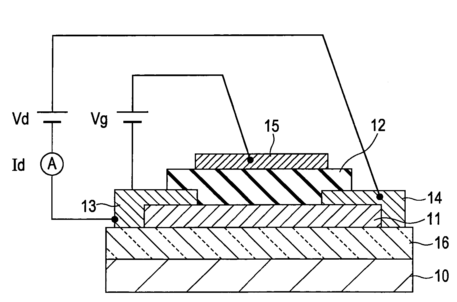
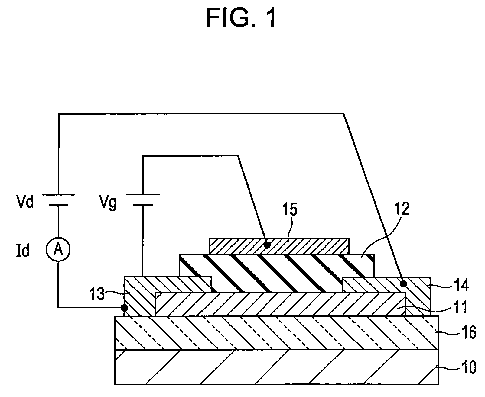
[0089]In EXAMPLE 1, a top-gate TFT shown in FIG. 1 is fabricated.

[0090]A transparent layer 16 of an amorphous oxide film is formed on a glass substrate having a refractive index of about 1.5.

[0091]In this EXAMPLE, an amorphous oxide film of the InGaZnO system is formed by high-frequency sputtering in an atmosphere of a mixture of argon and oxygen.

[0092]The InGaZnO system amorphous oxide film is formed by simultaneously sputtering three targets (2 inches in diameter) of In2O3, Ga2O3, and ZnO at radio-frequency (RF) powers of 15 W, 200 W, and 25 W, respectively. The atmosphere during the film-forming process has a total pressure of 0.4 Pa. The gas flow ratio of Ar and O2 is 100:2. The temperature of the substrate is 25° C.

[0093]The resulting thin film is evaluated by spectroscopic ellipsometry to confirm that the thickness is 75 nm and the refractive index at a wavelength of 550 nm is about 1.9. The thin film is confirmed to be insulative by the evaluation of the resistivity of the fi...

example 2

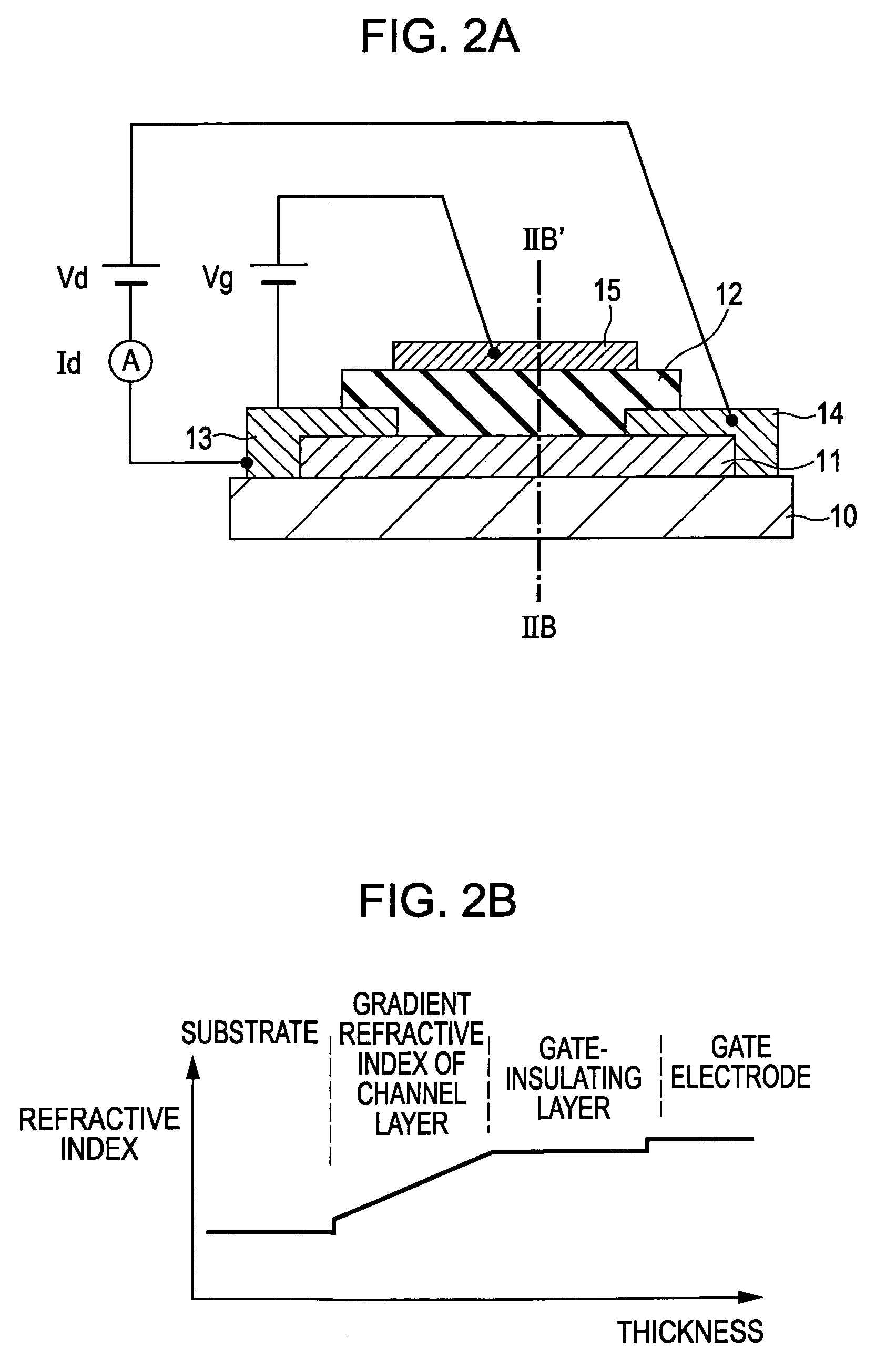
[0111]In EXAMPLE 2, a top-gate TFT shown in FIGS. 2A and 2B is fabricated on a plastic substrate. In the device of this EXAMPLE, the channel layer is a film having a gradient refractive index.

[0112]Firstly, a channel layer of an amorphous oxide film is formed on a polyethylene terephthalate (PET) film having a refractive index of about 1.5.

[0113]In this EXAMPLE, the amorphous oxide film of the InGaZnO system is formed by high-frequency sputtering in an atmosphere of a mixture of argon and oxygen.

[0114]The InGaZnO system amorphous oxide film is formed by simultaneously sputtering three targets (2 inches in diameter) of In2O3, Ga2O3, and ZnO.

[0115]The RF powers applied to the targets, In2O3, Ga2O3, and ZnO, are 0 W, 200 W, and 0 W, respectively, when the film-forming starts. Then, the RF powers applied to the In2O3 and ZnO are increased and the RF power applied to the Ga2O3 is decreased. Finally, all the RF powers applied to the In2O3, Ga2O3, and ZnO are 40 W. The atmosphere during th...

example 3

[0123]FIG. 8 is a cross-sectional view showing a structure of a thin-film diode in EXAMPLE 3 according to the present invention.

[0124]In EXAMPLE 3, as an oxide semiconductor device, a PN-junction device (thin-film diode) having a structure shown in FIG. 8 is fabricated.

[0125]Firstly, a transparent layer 16 of an InGaZnO system amorphous oxide film is formed on a glass substrate 10 having a refractive index of about 1.5. In this EXAMPLE, the film is formed by sputtering an In2O3.Ga2O3.ZnO oxide composite target. The atmosphere during the film-forming process has a total pressure of 0.4 Pa. The gas flow ratio of Ar and O2 is 100:10. The temperature of the substrate is 25° C.

[0126]The resulting thin film is evaluated by spectroscopic ellipsometry to confirm that the thickness is 75 nm and the refractive index at a wavelength of 550 nm is about 1.9.

[0127]The composition of the thin film by fluorescence X-ray analysis is In:Ga:Zn=1:1:0.9.

[0128]Then, an n-type semiconductor layer 21 of an...


PUM


Abstract

A thin-film transistor including a channel layer being formed of an oxide semiconductor transparent to visible light and having a refractive index of nx, a gate-insulating layer disposed on one face of the channel layer, and a transparent layer disposed on the other face of the channel layer and having a refractive index of nt, where there is a relationship of nx>nt. A thin-film transistor including a substrate having a refractive index of no, a transparent layer disposed on the substrate and having a refractive index of nt, and a channel layer disposed on the transparent layer and having a refractive index of nx, where there is a relationship of nx>nt>no.

Description

BACKGROUND OF THE INVENTION[0001]1. Field of the Invention[0002]The present invention relates to transparent semiconductor devices. Specifically, the present invention relates to field-effect thin-film transistors and thin-film diodes having amorphous-oxide semiconductor-layers.[0003]2. Description of the Related Art[0004]Field-effect transistors (FETs) are three-terminal devices each having a gate electrode, a source electrode, and a drain electrode. An FET is an electronically active device for switching a current between the source electrode and the drain electrode by applying a voltage to the gate electrode to control the current flowing in a channel layer. In particular, an FET having a channel layer of a thin film disposed on an insulating substrate of ceramics, glass, or plastic is called a thin-film transistor (TFT).[0005]TFTs are fabricated by using thin-film technology and advantageously can be readily formed on a substrate having a relatively large area. Therefore, TFTs a...

Claims


Application Information

Patent Timeline
Patent Type & Authority Patents(United States)
IPC IPC(8): H01L29/04H01L21/336H01L29/786H01L29/861H01L29/868
CPCH01L29/7869
Inventor IWASAKI, TATSUYA
Owner CANON KK
Why Eureka
Try Eureka