
Semiconductor memory device

a memory device and semiconductor technology, applied in the field of semiconductor memory devices, can solve the problems of insufficient dedicated dsp to achieve dramatic improvement in performance, increase in processing time proportionally, and become difficult to achieve high speed processing, etc., and achieve the effect of high speed

Active Publication Date: 2008-12-09
RENESAS ELECTRONICS CORP
View PDF7 Cites 30 Cited by
  • Summary
  • Abstract
  • Description
  • Claims
  • Application Information

AI Technical Summary

Benefits of technology

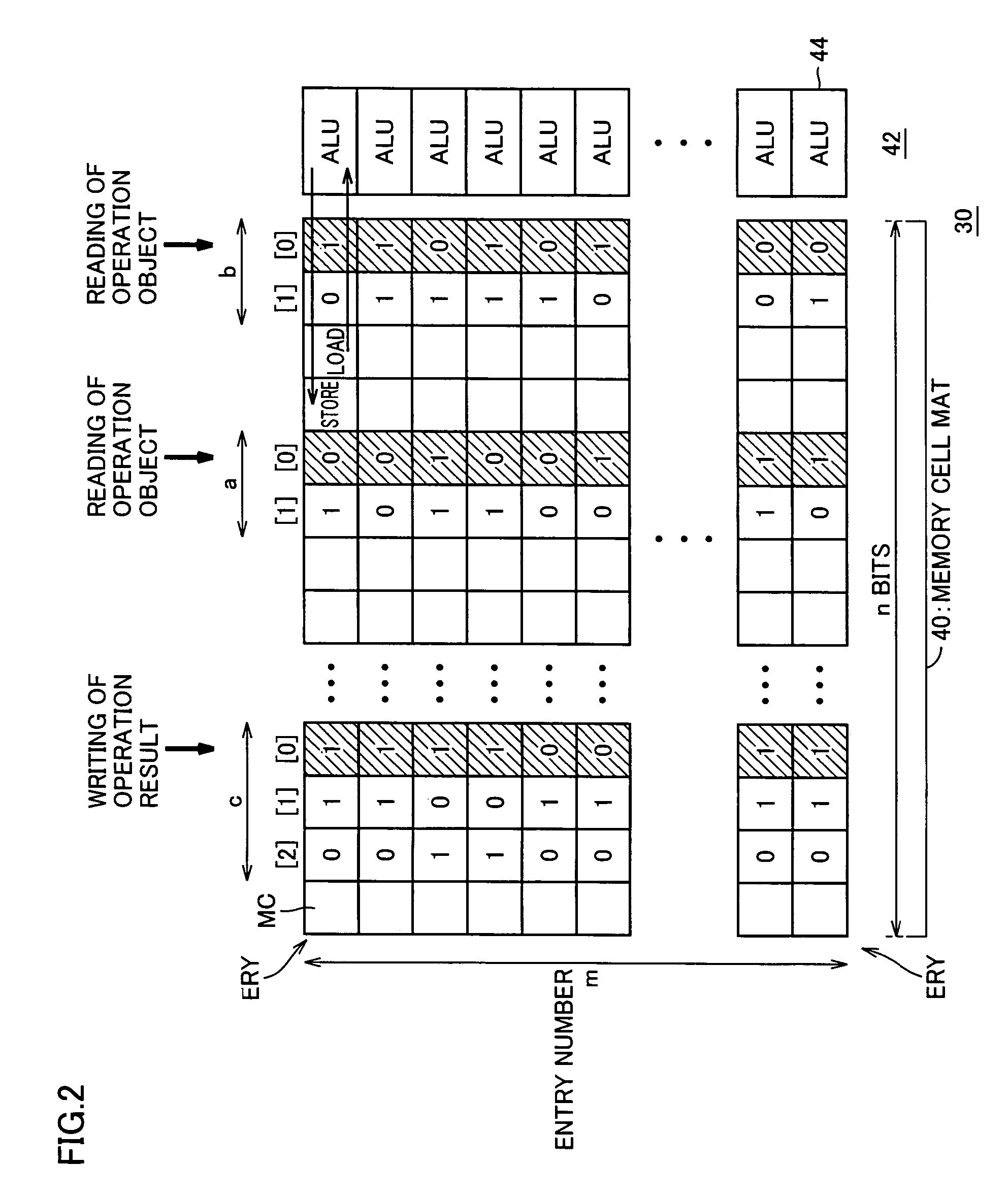
The present invention provides a semiconductor memory device that can transform data arrangement and transfer data at high speed. It includes a memory cell with a data storage portion and a search / read portion driving a match line pair in response to the potential of a search line and in accordance with the data stored in the data storage portion. The data storage portion reads the stored data to the bit lines and the match line pair, when the first and second word lines are selected, respectively. The memory cell also includes a pair of search lines that can be used as the transfer path for complementary data, reducing the number of signal lines for the memory cell. The first and second word lines are arranged to cross each other, allowing change in arrangement of memory cells connected to the selected word line, and hence, allowing transformation of the sequence of bit arrangement of the input / output data. The search line pair can mask a data write at the destination of data transfer, allowing data arrangement to be transformed without impairing the write mask function. It also allows for parallel operation only on the necessary data, suppressing degradation in operation speed.

Problems solved by technology

Therefore, when the amount of data to be processed is very large, even a dedicated DSP is insufficient to achieve dramatic improvement in performance.
Therefore, when data are processed serially using a dedicated DSP and the amount of data increases, the time of processing increases in proportion thereto, and therefore, it becomes difficult to achieve high speed processing.
When the data read from the CAM cell is to be stored at a transfer destination, it is impossible to mask the data writing of transferred data bits at the destination.
Consequently, the precharge voltage level of the bit line differs in data reading / writing and in a searching operation, and therefore, voltage control of the bit line is complicated.
Thus, it becomes difficult to select at high speed a memory cell and transfer data between the operating portion and the memory cell, hindering high speed processing.
Further, References 1 and 2 do not address how to execute parallel processing when the data of the object of processing have different word configurations.

Method used


Image

  • Semiconductor memory device
  • Semiconductor memory device
  • Semiconductor memory device

Examples


embodiment 1

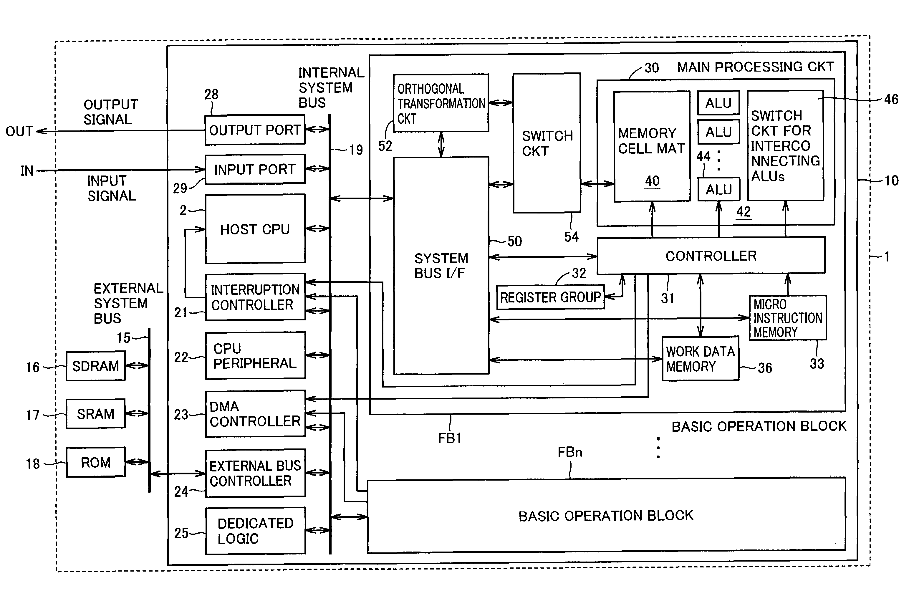
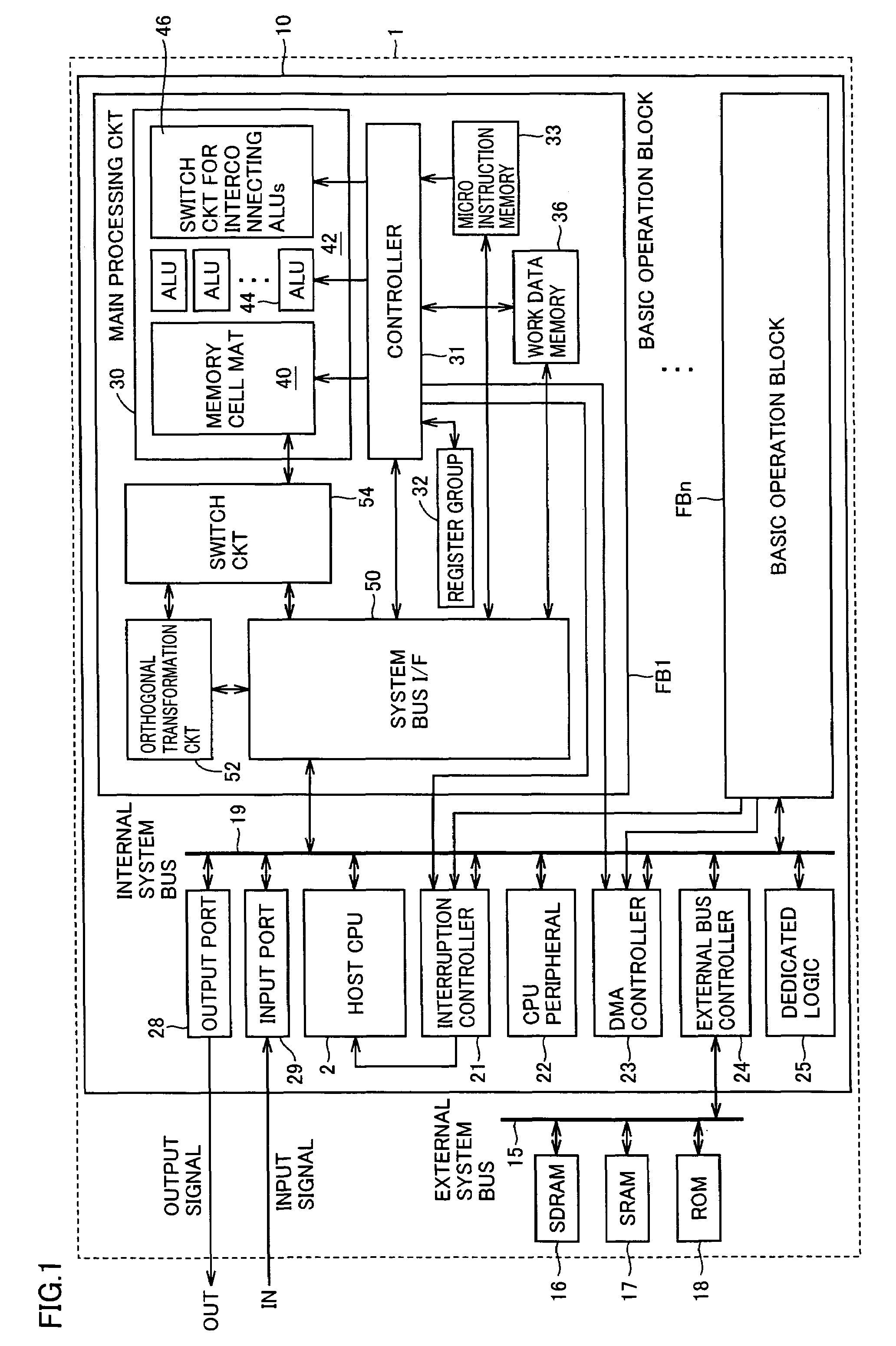
[0064]FIG. 1 schematically shows an overall configuration of a semiconductor signal processing system to which the semiconductor memory device of the present invention is applied. Referring to FIG. 1, a signal processing system 1 includes a system LSI 110 implementing arithmetic / logic operation functions for executing various processes, and external memories connected to system LSI 110 through an external system bus 15.

[0065]The external memories include a large capacity memory 16, a high-speed memory 17 and a read only memory (ROM) 18 storing fixed information such as an instruction for starting up the system. Large capacity memory 16 is formed, for example, of a clock-synchronized dynamic random access memory (SDRAM). High-speed memory 17 is formed, for example, of a static random access memory (SRAM).

[0066]System LSI 110 has, for example, an SOC (System On Chip) configuration, and includes basic operation blocks FB1 to FBn coupled in parallel with an internal system bus 19, a hos...

embodiment 2

[0217]FIG. 21 shows a configuration of a memory cell MCC of a semiconductor memory device in accordance with Embodiment 2 of the present invention. Referring to FIG. 21, memory cell MCC includes: an information data storage portion 200 for storing complementary data; a mask data storage portion 201 storing mask data inhibiting writing of data stored in information data storage portion 200 to the memory cell mat in the main processing circuitry; search / read gates 202a and 202b for driving match lines MLT[i] and MLB[i] in accordance with signals on search lines SLB[j] and SLT[j] and the data stored in data storage portion 200; a horizontal write port 204 for coupling storage nodes SNDT and SNDB of data storage portion 200 to match lines MLB[i] and MLT[i], respectively, in accordance with a signal on horizontal word line HWLT[j]; and a horizontal write port 205 for coupling storage nodes SNBT and SNBB of mask data storage portion 201 to match lines MLB[i] and MLT[i], respectively, in a...

embodiment 3

[0242]FIG. 26 shows a configuration of memory cell MCC in accordance with Embodiment 3 of the present invention. Memory cell MCC shown in FIG. 26 differs from the memory cell MCC in accordance with Embodiment 1 shown in FIG. 8 in the following points. Specifically, search / read gates 104a and 104b receive potential on bit lines VBLTB[j] and VBLBB[j] as search data, respectively, and selectively drive match lines MLT[i] and MLB[i] in accordance with the stored data, respectively. Specifically, search lines SLT[j] and SLB[j] are omitted, and bit lines VBLTB[j] and VBLBB[j] are used as the search lines and vertical bit lines. Thus, the number of signal lines for the memory cell MCC can be reduced, the interconnection area of the memory cells can be reduced and the layout area of the memory cell can be reduced.

[0243]Configurations of data storage portions 100a and 100b are the same as data storage portions 100a and 100b of memory cell MCC shown in FIG. 8, and therefore, corresponding por...


PUM


Abstract

A CAM (Content Addressable Memory) cell includes first and second data storage portions storing data, horizontal port write gates for storing data applied through a match line pair in the data storage portions in a data write through a horizontal port, and search / read gates for driving the match lines of the match line pair in accordance with the data stored in the data storage portions in a search operation and in a data read through the horizontal port. The match lines are used as horizontal bit line pair, or signal lines for accessing the horizontal port. As the first and second data storage portions are used, it becomes possible to store ternary data, and accordingly, a write mask function of inhibiting a data write at a destination of data transfer is realized. Further, as the CAM cell is used, an arithmetic / logic operation following a search process can be executed selectively, and high speed data writing / reading becomes possible.

Description

BACKGROUND OF THE INVENTION[0001]1. Field of the Invention[0002]The present invention relates to a semiconductor memory device and, specifically, to a content addressable memory (CAM) storing ternary data. More specifically, the present invention relates to a CAM having an orthogonal transformation function of transposing rows and columns of a multi-bit data arrangement.[0003]Particularly, the present invention relates to a semiconductor memory device realizing the orthogonal transformation function of transforming arrangement between external data and the processed data, in a semiconductor signal processing device having a parallel operation processing function.[0004]2. Description of the Background Art[0005]Recently, along with wide spread use of portable terminal equipment, digital signal processing allowing high speed processing of a large amount of data such as voice and image comes to have higher importance. For such digital signal processing, generally, a DSP (Digital Signal ...

Claims


Application Information

Patent Timeline
Patent Type & Authority Patents(United States)
IPC IPC(8): G11C7/00
CPCG11C15/00G11C15/04
Inventor DOSAKA, KATSUMIARIMOTO, KAZUTAMISAITO, KAZUNORINODA, HIDEYUKI
Owner RENESAS ELECTRONICS CORP
Learn More