Bistable nematic liquid crystal device

a liquid crystal device and nematic technology, applied in non-linear optics, instruments, optics, etc., can solve the problems of poor switching performance, lack of contrast, reflectivity, inefficiency of power usage, etc., to improve device performance, reduce scattering, and improve the effect of “dark” sta

Active Publication Date: 2008-12-30
ZBD DISPLAY LTD +1
View PDF21 Cites 43 Cited by
  • Summary
  • Abstract
  • Description
  • Claims
  • Application Information

AI Technical Summary

Benefits of technology

[0033]Improved contrast is also possible by matching the ordinary refractive index of the liquid crystal to that of the grating material (e.g. photo-resist). This helps reduce scattering in the continuous st

Problems solved by technology

Common problems to many conventional liquid crystal display devices includes narrow angle of view, lack of contrast, and reflectivity, poor switching performance, in

Method used


Image

  • Bistable nematic liquid crystal device
  • Bistable nematic liquid crystal device
  • Bistable nematic liquid crystal device

Examples


example 2

[0139]A similar cell to that of example 2 was also produced but this time using zinc-sulphide substrates rather than the conventional glass. This cell was then tested for use in the IR by imaging a warm object using an IR camera sensitive to the wavelength range 3 to 5 μm. The contrast between scattering and non-scattering states was found to be significantly higher than that observed at optical wavelengths, so that an image, which was clearly discernible in the non-scattering state, was obscured by the cell after latching into the scattering state.

example 3

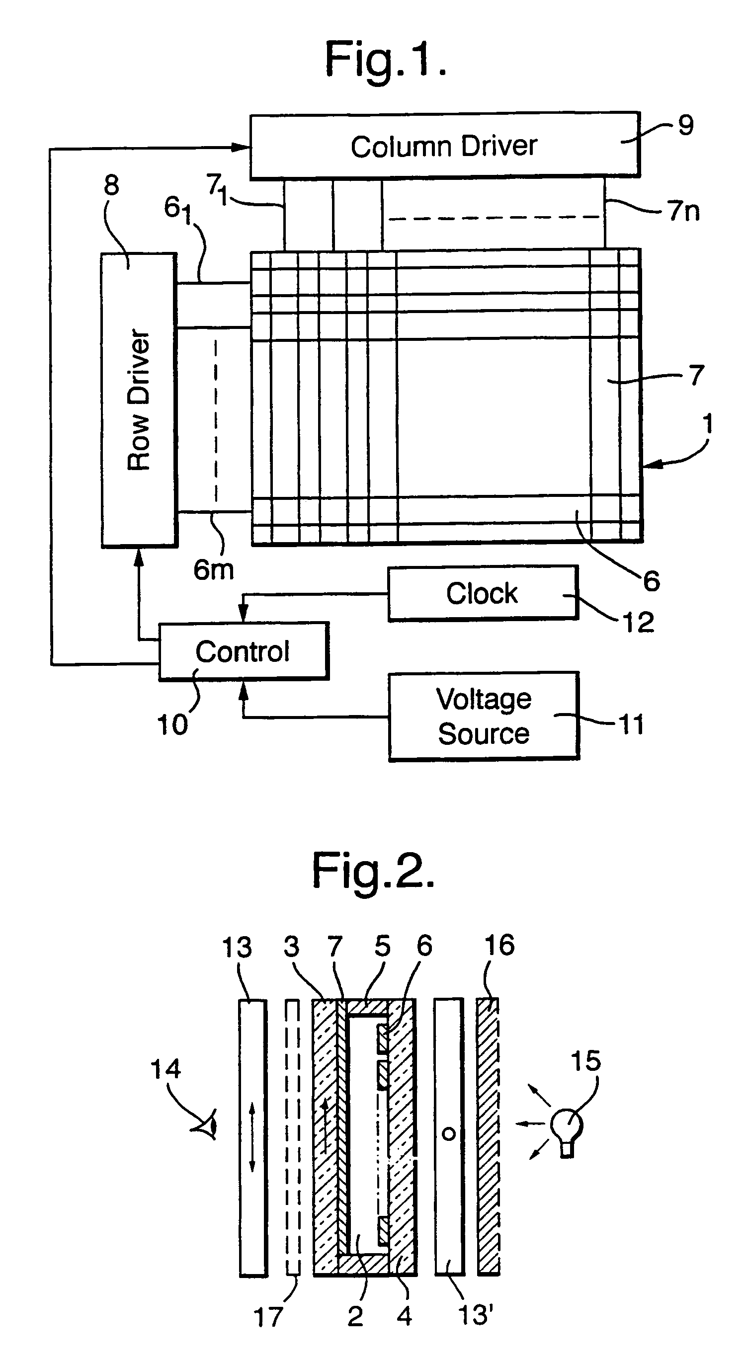
[0140]A third cell was prepared following the same procedure as in the previous example, but the cell was filled with the liquid crystal E7 into which 2% by weight of a black dichroic dye had been mixed (see for example Bahadur Liquid Crystals: Applications and Uses, Volume 3, Chapter 11, World Scientific Press). In this case, a contrast ratio of about 2:1 was observed between the two latched states for light of normal incidence, due to the difference in optical absorption between the two states. This was improved still further by operating the cell in reflective mode, in which the flat surface of one side of the cell was coated by a reflective aluminium layer.

example 4

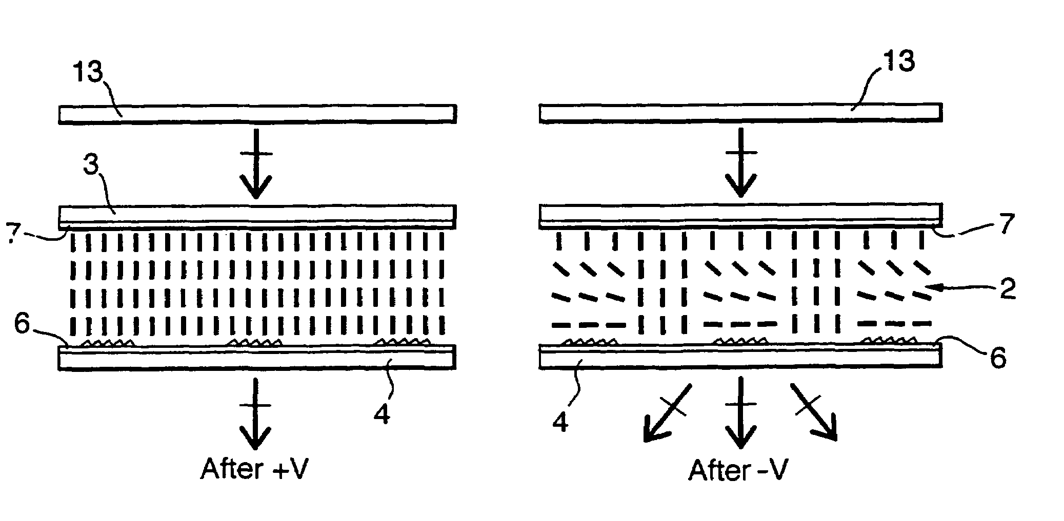
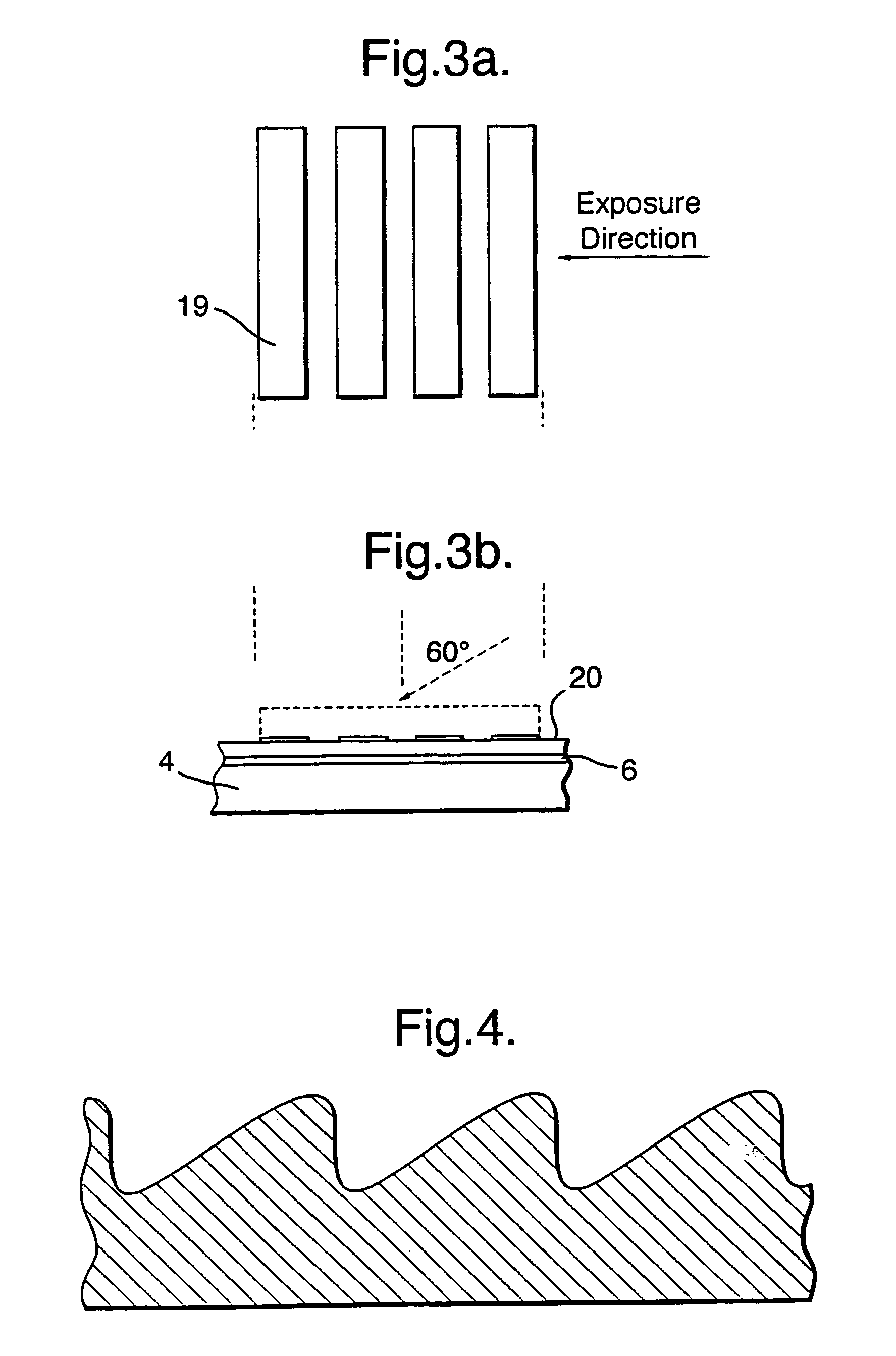
[0141]In the previous example, the scattering was very weak, and unattractive for a display device. The reason for this was that the size of the variation of alignment direction within the substrate plane was on length scales significantly higher than the wavelength of incident light. To ensure a higher degree of scattering for optical wavelengths a substrate was prepared using a mask with a design similar to that of FIG. 6b), wherein the grating pitch was 0.15 μm and the features of constant groove direction had an average width of about 0.6 μm. The smaller feature sizes were achieved using a frequency doubled argon ion laser (at 257 nm, for example see Hutley ibid p 99) used to develop the deep UV photo resist PMGI. In this example, the substrate was irradiated at normal incidence. After development, the surface was coated with a fluorinated chrome complex homeotropic surfactant and spaced at 20 μm from a second, flat homeotropic surface. The cell was again filled with BLO36, as i...


PUM


Abstract

A liquid crystal device comprises a layer (2) of a nematic liquid crystal material contained between two cell walls (3, 4) each carrying electrode structures (6, 7) and an alignment surface (20, 21). The alignment layer (20, 21) on one or both cell wall (4), is formed of a plurality of small (<15 μm) surface features each separably capable of providing a bistable pretilts and an alignment direction and collectively causing larger variations of molecular orientation across the layer (2). The device may be switched between a light transmissive state and a light non-transmissive state. The small surface features may be areas of grating (21), protrusions (25), or blind holes (26), separated by mono stable flat surfaces (Fm) coated with a homeotropic alignment layer. Preferably, the grating etc provides bistable switching operation between a low surface tilt and high surface tilt, and the low tilt alignment direction varies between adjacent grating areas.

Description

[0001]This application is a U.S. national phase of PCT / GB00 / 04447, filed on Nov. 23, 2000, claiming priority from GB 9928126.3, filed on Nov. 30, 1999, the entire contents of which are hereby incorporated by reference in this application.[0002]This invention relates to liquid crystal devices, in particular modulation devices operating with either a single polariser or with no polariser in which modulation occurs by virtue of diffraction, scattering or absorption of incident light.DESCRIPTION OF THE PRIOR ART[0003]Liquid crystal devices typically comprise a thin layer of liquid crystal material contained between cell walls, at least one of which is optically transparent. These walls are typically coated on the internal surface with transparent conducting layers to enable external electric fields to be applied. The electrodes are often formed as a series of strips forming row or line electrodes on one wall and columns on the other wall. The intersections of rows and columns give a xy ...

Claims


Application Information

Patent Timeline
IPC IPC(8): G02F1/1337G02F1/139
CPCG02F1/133753G02F1/13378G02F1/1391G02F1/1392G02F2001/133742G02F2001/133757G02F2001/133761G02F2201/30G02F2203/03G02F1/133742G02F1/133761G02F1/133757G02F1/133
Inventor JONES, JOHN C
Owner ZBD DISPLAY LTD
Why Eureka
Try Eureka