Semiconductor device and method for manufacturing same

a semiconductor and ohmic electrode technology, applied in semiconductor devices, diodes, electrical devices, etc., can solve the problems of low doping concentration, low breakdown voltage, and difficulty in obtaining an ohmic electrode at a doping concentration of 10sup>17 /sup>cmsup>3 , to achieve the effect of low loss, low breakdown voltage and low contact resistance of the source electrod

Inactive Publication Date: 2009-03-24
PANASONIC CORP
View PDF16 Cites 134 Cited by
  • Summary
  • Abstract
  • Description
  • Claims
  • Application Information

AI Technical Summary

Benefits of technology

[0012]The present invention is made to solve these problems, and its object is to realize a semiconductor device which keeps the contact resistance of a source electrode low without forming a source region by ion implantation and has a high breakdown voltage and low loss.
[0014]Therefore, even when a doped layer such as source and drain regions is not provided by ion implantation, a semiconductor device serving as a transistor or a diode allowing carriers to flow through the active region composed of a compound semiconductor can be realized. Accordingly, for semiconductor devices using compound semiconductors and having high performance such as high power and high breakdown voltage, their fabrication cost can be reduced.
[0018]When the compound semiconductor layer is a SiC layer, ion implantation requiring a large amount of labor particularly for the SiC layer need not be performed while advantage is taken of a large band gap. Therefore, the effect of reduction in fabrication cost becomes remarkable.
[0021]According to this method, a semiconductor device having an active region through which a large amount of carriers flow at a high speed can be obtained in the step (c) without ion implantation steps. More particularly, for semiconductor devices using compound semiconductors and having high performance such as high power and high breakdown voltage, their fabrication cost can be reduced.

Problems solved by technology

However, in this case, the breakdown voltage decreases.
Therefore, the impurity concentration in the accumulation channel layer cannot be high.
However, the document says that since the contact resistance of the ohmic electrode varies greatly depending on the doping concentration of silicon carbide, it is difficult to obtain an ohmic electrode at a doping concentration of 1017 cm−3 or less.
However, the structure of the known semiconductor device has the following problems.
This makes it difficult to clear crystal defects formed therein due to ion implantation.
In this case, defects may cause troubles.
In turn, the fabrication process is complicated, resulting in increased cost.
However, when annealing is conducted at 1500° C. or higher, silicon is selectively evaporated from the surface of SiC to form pits or cause step bunching, and flatness of the surface is degraded.

Method used


Image

  • Semiconductor device and method for manufacturing same
  • Semiconductor device and method for manufacturing same
  • Semiconductor device and method for manufacturing same

Examples


embodiment 1

[0042]“Structure of Semiconductor Device”

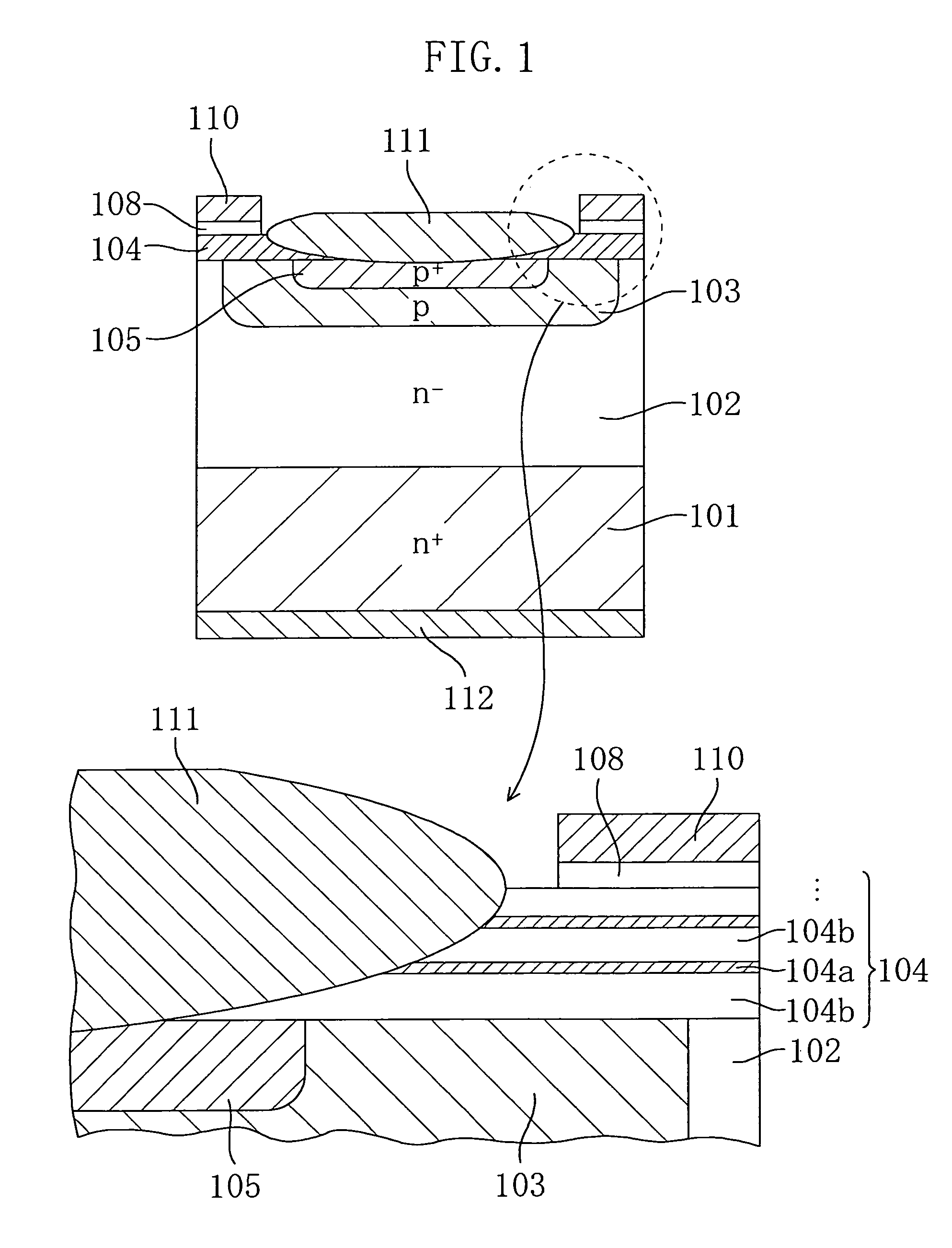
[0043]FIG. 1 is a cross sectional view showing a double-implanted, accumulation-mode MISFET (ACCUFET) using SiC according to a first embodiment of the present invention.

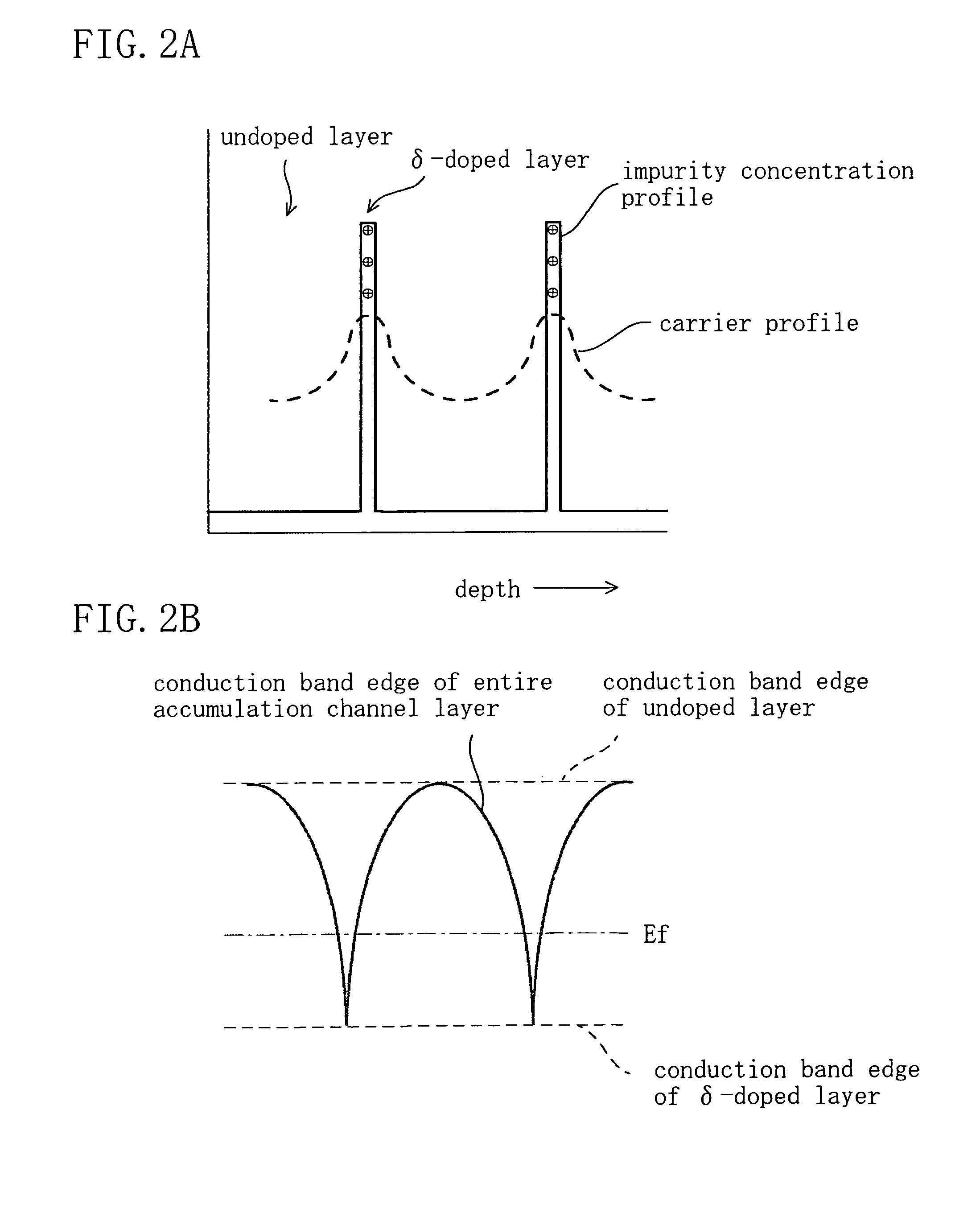
[0044]As shown in this figure, an accumulation-mode MISFET of this first embodiment comprises a low-resistance SiC substrate 101, a high-resistance SiC layer 102 that is epitaxially grown on the SiC substrate 101 and has a higher resistance than the SiC substrate 101, a p-type well region 103 formed by selectively implanting ions into the surface region of the high-resistance SiC layer 102, an n-type accumulation channel layer 104 having a multiple δ-doped layer (active region) formed on the surface region of the well region 103, and a contact layer 105 formed by implanting a p-type impurity at a high concentration into the well region 103. A gate insulating film 108 is formed on the accumulation channel layer 104, and a gate electrode 110 is formed on the gate insulating film...

embodiment 2

[0075]“Structure of Semiconductor Device”

[0076]FIG. 4 is a cross sectional view showing the structure of a trench MISFET constituting a semiconductor device according to a second embodiment of the present invention.

[0077]As shown in this figure, a trench MISFET of this second embodiment comprises a low-resistance SiC substrate 201, a high-resistance SiC layer 202 that is epitaxially grown on the SiC substrate 201 and has a higher resistance than the SiC substrate 201, a p-type base layer 203 formed by selectively implanting ions into the surface region of the high-resistance SiC layer 202, an n-type channel layer 204 having a multiple δ-doped layer (active region) formed along the wall surface of a trench which passes through part of the p-type base layer 203 and reaches the high-resistance SiC layer 202, and a contact region 205 formed by implanting a p-type impurity at a high concentration into the p-type base layer 203. A gate insulating film 208 is formed on the channel layer 20...

embodiment 3

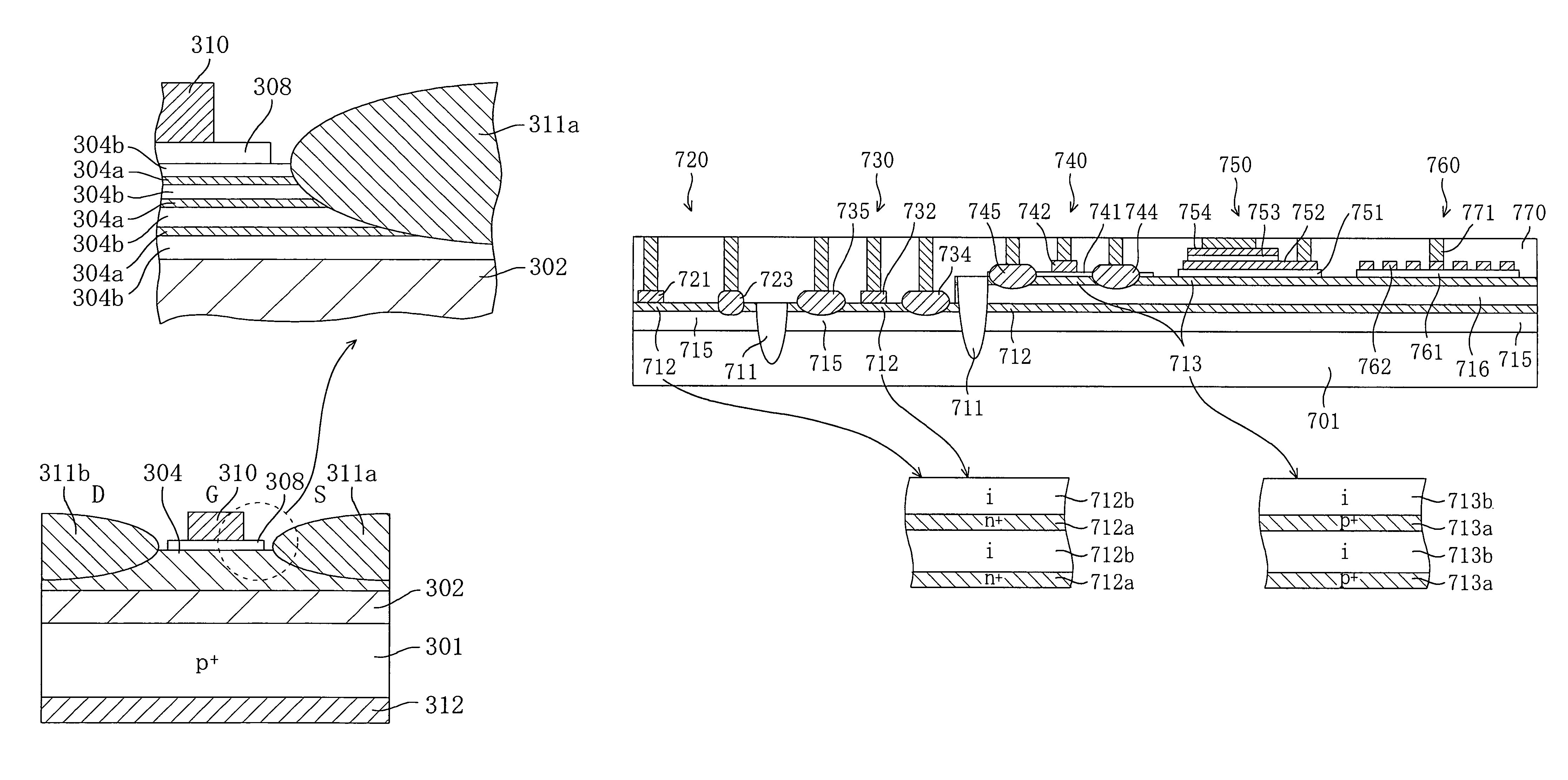
[0099]FIG. 6 is a cross sectional view showing a schematic structure of a lateral p-channel MISFET according to a third embodiment. As shown in this figure, on an n-type SiC substrate 301 doped with nitrogen (n-type impurity) at a concentration of 1×10¹⁸ atoms·cm−3, there are provided an n-type base region 302 doped with nitrogen at a mean concentration of about 1×10¹⁷ atoms—cm−3, a multiple δ-doped layer 304 (active region) formed in the base region 302, a gate insulating film 308 of SiO2 formed on the multiple δ-doped layer 304, a gate electrode 310 composed of a Ni alloy film formed on the gate insulating film 308, source and drain electrodes 311a and 311b composed of a Ni alloy film contacting the multiple δ-doped layer 304 and the base region 302, and a back-surface electrode 312 composed of a Ni alloy film in ohmic contact with the back surface of the SiC substrate 301.

[0100]As shown in the right part of FIG. 6 under magnification, the multiple δ-doped layer 304 is composed of...


PUM


Abstract

An accumulation-mode MISFET comprises: a high-resistance SiC layer 102 epitaxially grown on a SiC substrate 101; a well region 103; an accumulation channel layer 104 having a multiple δ-doped layer formed on the surface region of the well region 103; a contact region 105; a gate insulating film 108; and a gate electrode 110. The accumulation channel layer 104 has a structure in which undoped layers 104b and δ-doped layers 104a allowing spreading movement of carriers to the undoped layers 104b under a quantum effect are alternately stacked. A source electrode 111 is provided which enters into the accumulation channel layer 104 and the contact region 105 to come into direct contact with the contact region 105. It becomes unnecessary that a source region is formed by ion implantation, leading to reduction in fabrication cost.

Description

TECHNICAL FIELD[0001]The present invention relates to a semiconductor device formed using a compound semiconductor layer, and more particularly relates to a semiconductor device suitable for applications requiring a high breakdown voltage or a large current, and a method for fabricating the same.BACKGROUND ART[0002]Among various semiconductor devices, power devices are required to have a high breakdown voltage and handle a large current while achieving low loss. Although power devices using silicon (Si) semiconductors have conventionally been in common use, attention has in recent years been focused on power devices using compound semiconductors having a wide band gap, such as silicon carbide (SiC). Such compound semiconductor power devices are now being developed. In particular, silicon carbide semiconductors have a dielectric breakdown electric field ten times greater than silicon, and thus can maintain a relatively high reverse breakdown voltage in spite of a narrow depletion lay...

Claims


Application Information

Patent Timeline
Patent Type & Authority Patents(United States)
IPC IPC(8): H01L21/00H01L29/15H01L31/0312H01L21/04H01L21/336H01L21/28H01L21/338H01L21/82H01L21/822H01L21/8232H01L21/8234H01L27/04H01L27/06H01L27/095H01L29/12H01L29/24H01L29/36H01L29/45H01L29/47H01L29/772H01L29/78H01L29/812H01L29/872
CPCH01L21/0485H01L21/8213H01L27/0629H01L29/66068H01L29/7725H01L29/7813H01L29/7828H01L29/7838H01L29/812H01L29/872H01L27/0605H01L29/1029H01L29/105H01L29/1608H01L29/365H01L29/41766Y10S438/931
Inventor KUSUMOTO, OSAMUKITABATAKE, MAKOTOTAKAHASHI, KUNIMASAYAMASHITA, KENYAMIYANAGA, RYOKOUCHIDA, MASAO
Owner PANASONIC CORP
Why Eureka
Try Eureka