Radiation detection circuit and radiological imaging apparatus using the same

a radiological imaging and detection circuit technology, applied in the field of radiological imaging apparatus, can solve the problems of increasing time, reducing the effective count, and hardly practicable medical equipment for semiconductor detectors, so as to improve the contrast of diagnostic images and shorten the diagnostic imaging tim

Inactive Publication Date: 2009-05-05
HITACHI LTD
View PDF11 Cites 12 Cited by
  • Summary
  • Abstract
  • Description
  • Claims
  • Application Information

AI Technical Summary

Benefits of technology

[0004]Prior to this application, the applicants examined the timing signal generation technology in coincidence measurement (hereafter referred to as coincidence measurement) of proton and annihilation radiation. The measurement is needed for a radiological imaging apparatus using a radiation detector (hereafter referred to as a semiconductor detector) made of semiconductor devices. The proton is generated from a positron nuclide. The annihilation radiation has the same energy as 511 keV generated upon annihilation of an electron existing in a human body annihilates and travels 180□ reversely. Compared to a conventional scintillator, the radiological imaging apparatus using the semiconductor detector: 1) excels in detector-specific energy resolution, enables the simultaneous use of medicines containing multiple nuclides with different energies, and improves the image contrast; and 2) is capable of further miniaturizing a detector's physical shape, improving the space resolution compared to the conventional scintillator, and acquiring finer images. On the other hand, the semiconductor detector shows the following disadvantages. 1) The radiation stopping power is smaller than the conventional scintillator so that applying the same radiation dosage to a specimen decreases an effective count. 2) A position where the radiation enters the detector varies a generated signal waveform at a contribution ratio between electron transfer and hole transfer, causing a mobility difference ten times or more. The detection time deviation becomes up to 200 to 300 ns when a difference between generated current waveforms exceeds a given threshold level. This increases a probability of causing events that cannot be assumed to occur at the same time as timing data, decreasing the effective count. 3) Since the radiation stopping power is low, there is a high probability of scattering (hereafter referred to as Compton scattering distinguished from body scattering in the body water or bone) an incident radiation in the detector. The quantity of charge generated in the detector is irregular. Since the voltage waveform gradient changes with reference to an ideal signal waveform, the detection time varies with the energy to decrease the effective count. Generally, a timing window assumed to be the equal time approximately ranges from 10 to 20 ns for the coincidence measurement on the PET apparatus. When there is a detection timing difference of approximately 10 to 20 ns or smaller between two radiations traveling 180° opposite to each other, the two radiations are assumed to be detected at the same time. When the detection timing difference exceeds those values, the two radiations are not assumed to be detected at the same time even though they enter the semiconductor detector almost simultaneously. Such detection time variation greatly decreases a ratio of the number of events (hereafter referred to as the effective count) recognized to be the equal time. Accordingly, this greatly increases the time (diagnostics time for patients) to acquire data needed for the reconstruction. The semiconductor detector is hardly practicable as medical equipment and is therefore not commercialized. To solve this problem, FIG. 3 in JP-A No. 243858 / 2002 proposes a slew rate control circuit according to the timing signal generation technology.
[0009]The invention can shorten the diagnostics imaging time in the radiological imaging apparatus and improve the diagnostics image contrast.

Problems solved by technology

This increases a probability of causing events that cannot be assumed to occur at the same time as timing data, decreasing the effective count.
Accordingly, this greatly increases the time (diagnostics time for patients) to acquire data needed for the reconstruction.
The semiconductor detector is hardly practicable as medical equipment and is therefore not commercialized.
Further, it is difficult to correct process variations for each input signal.
The applicants originally found these problems of the prior art.

Method used


Image

  • Radiation detection circuit and radiological imaging apparatus using the same
  • Radiation detection circuit and radiological imaging apparatus using the same
  • Radiation detection circuit and radiological imaging apparatus using the same

Examples


embodiment 1

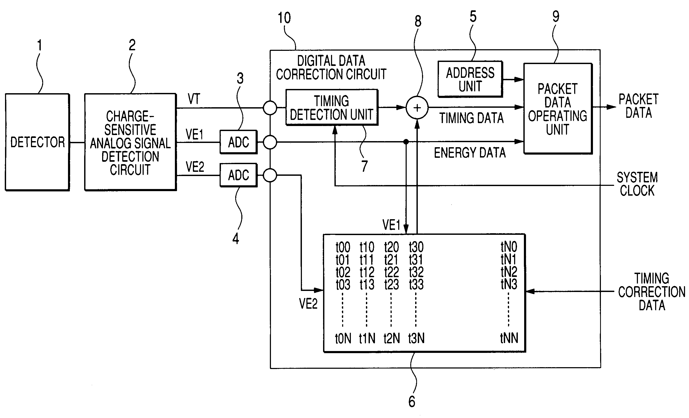
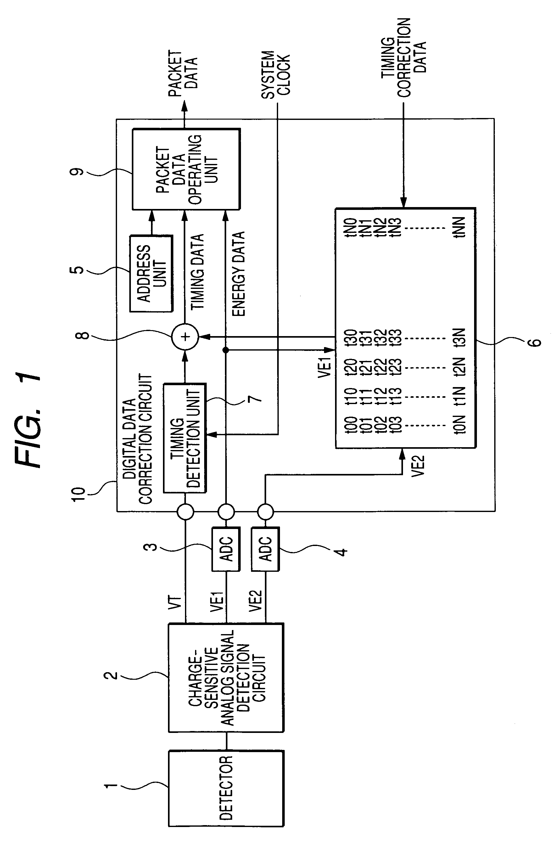
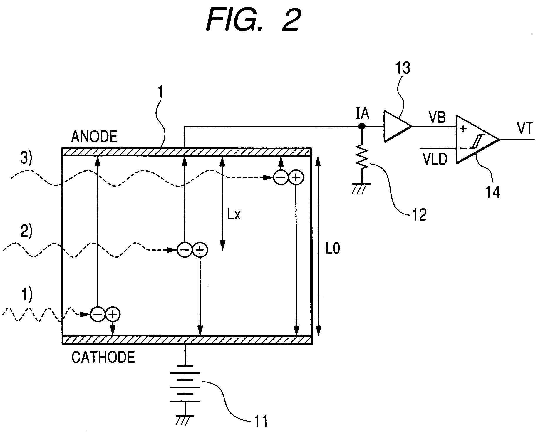
[0024]FIG. 1 shows a first embodiment of the radiation detection circuit in the PET / SPECT (Single Photon Emission Computed Tomography) apparatus as an example of the radiological imaging apparatus according to the invention. The PET / SPECT apparatus includes: a detector 1; a charge-sensitive analog signal detection circuit 2; analog / digital converters (ADCs) 3 and 4; and a digital data correction circuit 10. The digital data correction circuit 10 includes: a detector address unit 5; a timing correction data table unit 6; a timing detection unit 7 that converts a timing signal into timing data using a synchronized clock signal from the apparatus; a correction circuit 8; and a packet data generating unit 9. Generally, multiple detectors 1 are provided in the PET / SPECT apparatus so as to surround a test object. Each of all the detectors 1 is connected to the corresponding charge-sensitive analog signal detection circuit 2 on a one-to-one basis. The charge-sensitive analog signal detecti...

embodiment 2

[0043]FIG. 9 shows another embodiment of the construction of the timing correction data table unit 6 concerning the coincidence measurement in the radiological imaging apparatus using the semiconductor detector according to the invention. Embodiment 2 differs from embodiment 1 in that external memory is used for the timing correction data table unit 6 in the digital data correction circuit 10 according to embodiment 1. This aims at solving a problem where the table is too large to be stored in the digital data correction circuit 10. The PET / SPECT apparatus is composed of the detector 1, the charge-sensitive analog signal detection circuit 2, the analog / digital converters (ADCs) 3 and 4, the digital data correction circuit 10, and external memory 21. The digital data correction circuit 10 is composed of the detector address unit 5, the external memory control unit 20, a timing conversion circuit 7, the correction circuit 8, and the packet data generating unit 9. The timing conversion...

embodiment 3

[0045]FIG. 10 shows still another embodiment of the timing signal correction method concerning the coincidence measurement in the radiological imaging apparatus using the semiconductor detector according to the invention. Embodiment 3 differs from embodiment 1 in that the timing signal correction uses digital calculation instead of the table lookup method. That is, the timing correction data table unit 6 is replaced by a timing correction operating unit 22. The PET / SPECT apparatus is composed of the detector 1, the charge-sensitive analog signal detection circuit 2, the analog / digital converters (ADCs) 3 and 4, and the digital data correction circuit 10. The digital data correction circuit 10 is composed of the detector address unit 5, the timing correction operating unit 22, the timing conversion circuit 7, the correction circuit 8, and the packet data generating unit 9. The timing conversion circuit 7 converts a timing signal into timing data according to the clock signal synchron...


PUM


Abstract

There is a need for high-precision detection timing in a radiological imaging apparatus using a semiconductor detector so as to decrease time variations against a noise and easily correct process variations. A radiation detection circuit includes: a semiconductor detector; charge accumulation means connected to the semiconductor detector; a circuit to discriminate timing of a signal generated from the charge accumulation means based on a specified threshold value; a shaper 1 to limit a band from the charge accumulation means using a first time constant; a shaper 2 to limit a band from the charge accumulation means using a second time constant; a circuit 1 to hold an analog peak value 1 for the shaper 1; and a circuit 2 to hold an analog peak value 2 for the shaper 2. The radiation detection circuit performs a signal process to generate timing correction data based on the analog peak values 1 and 2 and correct timing data from the timing discriminator circuit.

Description

CLAIM OF PRIORITY[0001]The present application claims priority from Japanese patent application No. 2005-250521 filed on Aug. 31, 2005, the content of which is hereby incorporated by reference into this application.FIELD OF THE INVENTION[0002]The present invention relates to a radiological imaging apparatus such as a PET (Positron Emission Tomography) apparatus and a radiation detection circuit used for the apparatus. Specifically, the invention relates to a radiation detection circuit that reduces an error in detection timing dependent on positions for radiation to enter a semiconductor detector.BACKGROUND OF THE INVENTION[0003]Conventionally, there have been a radiation detection circuit and a radiological imaging apparatus for detecting simultaneously incident gamma rays at the same timing (see JP-A No. 243858 / 2002). In this case, a fast shaper and a slow shaper are supplied with electric signals detected by pixels. A current controller limits a timing signal formed by the fast s...

Claims


Application Information

Patent Timeline
Patent Type & Authority Patents(United States)
IPC IPC(8): G01T1/24
CPCG01T1/2928
Inventor MATSUMOTO, TAKASHI
Owner HITACHI LTD
Why Eureka
Try Eureka